


 tel:+86-18825224069
 email:
 address:201, Factory 6, Longhui Industrial Park, Fuqiao 3rd District, Xinhe Community, Fuhai Street, Baoan District, Shenzhen china
why you choose us?
The senior printed circuit board design engineering team participates in the whole process of your PCB design, from principle design, DFM, DFT, high-speed, EMC, thermal design and other comprehensive checks
-
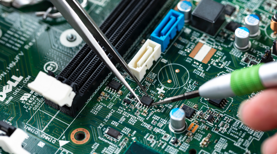
Senior PCBLayout design team
With more than 10 years of experience in PCB product design, we provide solutions from design to manufacturing. -
10+ years of experience
We have the experience and equipment needed to meet all your advanced PCB needs, from low-cost single-sided PCB to customized multi-layer PCB design and layout services. -
Excellent customer service team
We have a customer service team that provides customers with technical support, production operations and order services 24 hours a day, and can provide technical services online, telephone and e-mail.
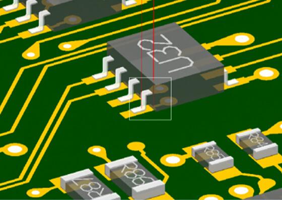
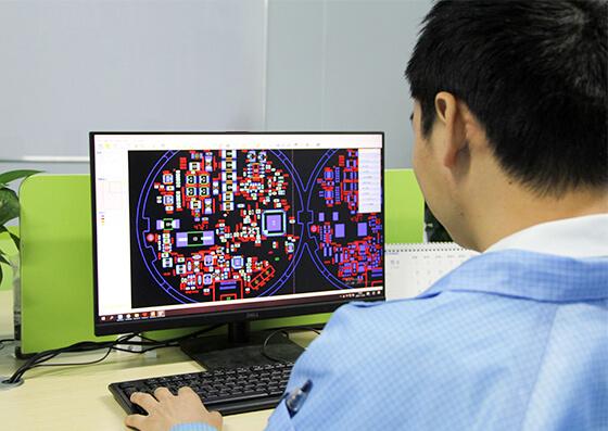
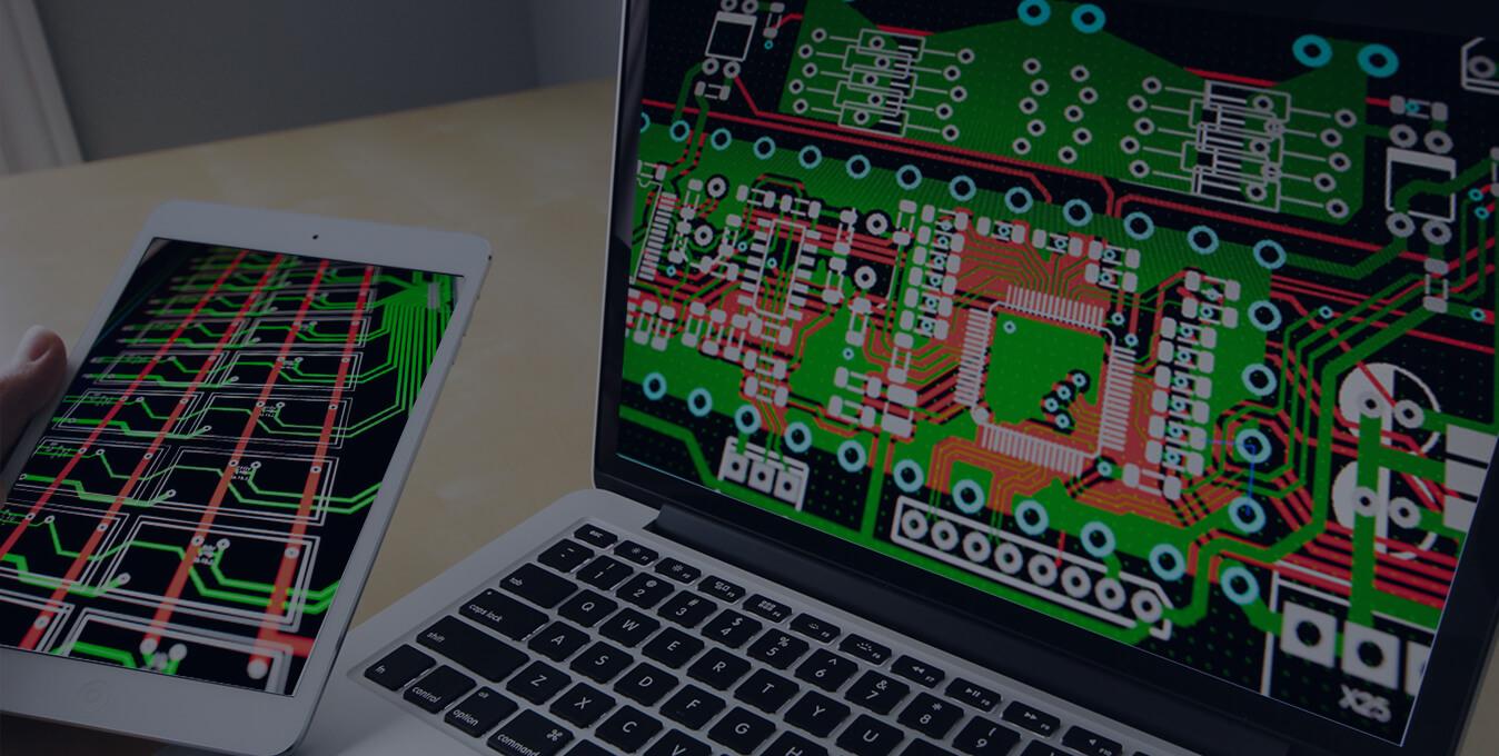
OUR PCB design capabilities
In the highly-competitive field of printed circuit board design, assembly, and fabrication, our designers understand that they must go the extra mile in order to win a customer’s business.
- Our full turn-key hardware design services include:
- Board Design and Layout:
- About KFPCBA
Design idea development, block diagram, power estimate
Schematic capture, BOM cost estimate
Enclosure/chassis design
PCB floor-plan study
PCB layout design
Thermal/Power Simulation
Power Integrity and Signal Integrity analysis
PCB fabrication and assembly
Board bring-up and testing
Hardware user manual, application notes
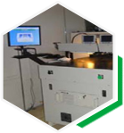
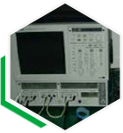
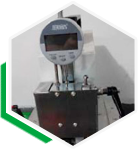
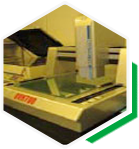
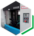
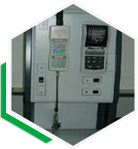
Testing and equipment
Our 30,000 sqm state-of-the-art campus in Shenzhen contains state-of-the-art equipment needed to manufacture and assemble PCBs. There's a reason KFPCBA leads the industry in both quality and performance.Contact Us 》
Quality certification
KFPCBA’s quality management system is designed to ensure that high-efficiency printed circuit boards meet customer requirements. Our partners produce according to the following standards, including:
Thanks to the use of materials and advanced technology, we always guarantee the highest quality printed circuit board!
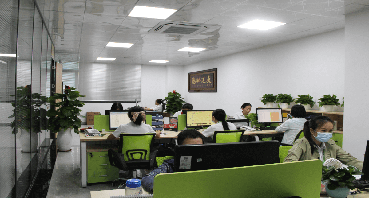
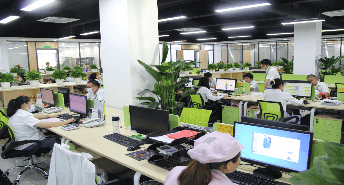
Our Workshop
Common problems of PCB design
-
1Can I make PCB samples after design?
We have our own PCB and SMT processing factories, which can satisfy customers with one-stop service from design to proofing
-
2How do I charge for PCB design
Generally 3-5RMB/PINS. This price provides invoices, contracts, confidentiality agreements, etc. Specific needs to be evaluated according to the difficulty of the product
-
3What design materials do PCB designs output to customers?
Design data output: PCB source files, Gerber files, assembly files, steel mesh files, structure files, etc.
-
4What does the design process include?
Design specifications, design instructions, customer design requirements and related CHECKLISTs, provide layout files, structure files for customers to conduct layout review; customers confirm the rationality of the layout, stacking scheme, impedance scheme, structure, packaging, and confirm the wiring parameters
-
5What information do I need to provide for PCB design?
The customer needs to provide information: schematic diagram, netlist, structure diagram, device data to be built in the library, design requirements, etc.
There are other questions?For more questions, please contact us >
Would you like us to design the PCB for you?
QuotationOur PCBA product demonstration
Do you need a quotation for your PCB Layout&Design ?
Leave us a message about your PCB Gerber production file or assembly BOM file! We will quote you today or tomorrow!


