


 tel:+86-18825224069
 email:
 address:201, Factory 6, Longhui Industrial Park, Fuqiao 3rd District, Xinhe Community, Fuhai Street, Baoan District, Shenzhen china
About slots and Cutouts:All the Details You Need for Your PCB Design
Release date:2022-09-19 17:56:45 Number of views:0
The PCB slot is a small but important detail of a PCB board. In the same way, a tremendous amount of detail goes into PCB designs for the appropriate PCB slot or cutouts. Many factors determine the function of these slots and cutouts.
So as a PCB manufacturer or enthusiast, you learn about PCB slots. You also know to customize your printed circuit board with the Cadence Padstack Editor. So, read on as we uncover the resources you need to become an expert PCB designer.
What is a PCB Slot?
A PCB slot is a large hole in a circuit board that cannot be created using standard PCB drilling techniques. To achieve this, manufacturers must use a routing bit to achieve these holes during PCB design. A PCB slot is either plated or non-plated.
Slots and Cutouts
Slots and cutouts come in different parts types and footprints. Some are plated, while others are non-plated. Their thru-hole assembly and component footprints often come as circular holes with square or circular leads. For example, the USB 2.0 port connector has a similar thru-hole configuration. Other slots and cutouts have parts with rectangular leads or blade-style holes. They work best for plated slot footprints.
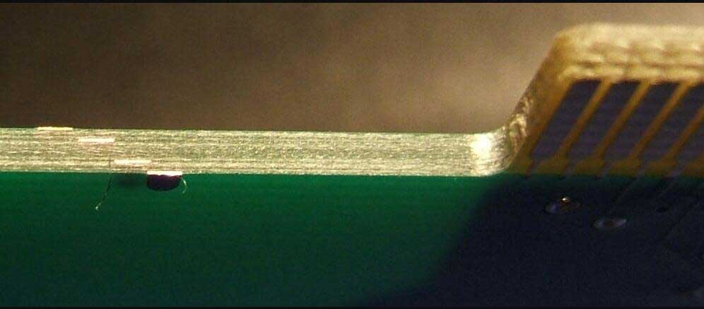
(An IC PCB with plated slots).
Types of PCB Slot
Your intent or purpose of use determines the type of PCB slot. The following are the slot types for your PCB design.
Plated slots
In general, Plated slots have copper plating. Also, it lacks a circular shape and is prevalent in multilayer printed circuit boards.
It is most useful in electrical connections and component packaging. In addition, their configuration matches the through-hole assemblies. These, in turn, enable its round slotted holes to fit in a round or square lead.
As the size of pins increases, the sizeable blade-style connector uses plated-through slots. That is, manufacturers feature rectangular pins with round holes for small parts. Though, round holes eventually occupy more circuit board space. Plated and non-plated slots are among the most popular in size-restricted designs.
Non-plated slots
On the other hand, non-plated slots have larger holes compared to the copper size of the pad. Sometimes, however, copper is absent. But then, the pad's copper overlays because the manufacturer does the electroless copper process before drilling the unplated slots.
Metallic Annular Slots
Typically, metalized plating is a process for drilling holes or slots found on a PCB copper foil. To add non-metal drill slots to a copper foil, define it with a new mechanical layer. Then, rename this new layer as "NPTH."
Non-Metallic Annular Slots
In most cases, adding a new non-metallic annular slot involves using a keep-out or mechanical layer. The automatic layer should have a 0.8mm line width defined as a slot. Otherwise, its dimension layer should have a marked-out box. Avoid using the silkscreen layer. When designing spaces with several complex designs, add a clear marker or picture to indicate specific areas.
The other PCB slots are the Half-Round Groove and Square Groove And Slot.
How to Define the Slot in PCB?
Mechanical Layer
The most preferred method for adding drilled slots or cutouts to a design is using them on a Gerber mechanical layer. It shows the PCB profile, the actual places, and cutouts in the most precise and safest ways possible. So, to define mechanical integrity:
Trace a 0.50mm line for the slots /cutouts. This line's center serves as the Slot's edge and helps gain better copper clearance of the PCB board edge. Use flashes or draws with the appropriate cutout or slot size.
Afterward, include your defined slots or cutouts alongside the PCB outline (PCB contour) inside the Gerber file. In the absence of a mechanical layer name, choose another layer. Otherwise, select a README file.
Do not define slots in legend layers or copper layers alone. It is easy to misunderstand or overlook them. Instead, ensure you mark them with a clear outline and the text "CUTOUT" down the center.
Drill File
CAD Software allows the definition of drill file slots. But it does not permit overlapping holes. Instead, it would help if you defined plot holes using X and Y dimensions.
Plated or Non-Plated
Plated slots or cutouts have copper on the top and bottom parts. Otherwise, they are non-plated slots and non-plated cutouts.
For non-plated slots, you must pull back the copper at a recommended length from the board edge DRC. It helps differentiate plated holes from non-plated holes in the design files. It also helps to indicate non-plated cutouts via copper pads in the mechanical layer, the file name, or a different drill file altogether.
What are the Applications of Slots in PCB?
So, to avoid long-term short circuits, PCB designers fabricate milling PCB slots for these suspect traces. Milling slots on a circuit board generate air space which helps voltage isolation. As a result, it prevents potential electrical arcs from high voltages and eventual PCB carbonation.
Slot footprints, in general, are better for large holes. Also, plated slots are the best for parts with rectangular leads or square leads, not rounded ones. That means you don't need extra solder on the information for it to fit the walls of the hole pad.
What is the Smallest Slot on PCBs?
Apart from the flex PCB, the minimum size slots on PCBs have a slot width of 0.5mm and a slot length of 1.0mm. Usually, a rigid-flex board and a plain rigid board have a dense thickness. Therefore, a mechanical NC milling machine forms the slots and cutouts on the PCB. The grooving cutter of the smallest NC machine has a 0.50mm diameter and is twice the dimension in length. On the other hand, Flex PCBs require a laser cut because they are thin.

(The laser-drilling process on a PCB).
Why Is The Minimum Annular Slot Not Equal to the Minimum Drill Hole?
During the printed circuit board fabrication, the milling slot process is responsible for forming the annular Slot. Unlike drilling tools, they are more prominent in diameter. In many cases, the minimum annular slot dimension is 0.8mm, while the minimum drill distance is 0.3mm. Therefore, milling tools deliver long annular slots and larger drill sizes.

(A CNC milling machine drilling PCB slots).
How to Create a Slot?
To begin, open Padstack Editor by clicking on the Windows icon. Next, navigate the menu by selecting Cadence PCB Utilities > Padstack Editor. > Choose File to name it.
Afterward, specify decimal places and units, change Padstack usage to Slot and activate a default pad geometry.
For example, you are working on an oval slot of 1mm by 2mm and a ±0.3mm drill tolerance.
First, you must choose the Drill Tab in the menu and select the slot type – Oval Slot. The diameter of the Slot is the Slot Y size, while the length is the Slot X size. Also, you need to adjust the X and Y tolerance values to ±0.3mm. Further, you need to specify whether it is a plated or non-plated slot. After entering the slot sizes, it gives you a preview.
Henceforth, select a drill symbol to define the character of the Slot you are creating. The figure size is in automatic default from slot X and Y sizes.
Next is to select the design layers tab to customize the design layers. These include the accurate pad sizes for your plated Slot.
However, when dealing with a mechanical layer slot, you must choose the solder mask layer from the mask layer tab.
Afterward, adjust the geometry from "None" in the Begin Layer to "Oblong."
Then, input the desired slot size, height, and width values. Offsets are also an option for the slot center and shape symbols in place of the pad geometry.
Further, you need to check the manufacturer's datasheet or the IPC 7251 standard to confirm your design matches your requirements.
After defining the Begin Layer, copy and paste to apply the default Inner and End Layers.
In the end, you also define the Paste mask and Solder mask to finish the pad designs.
Finally, the side and top views become visible from the Views tab. And the pad saves in the appropriate pad path library, ready for use.
Conclusion
PCB Slots are tiny drill holes that enable designers to attach peripherals to the finished circuit board. They often come as plated or non-plated, depending on the presence of copper.
There are several careful considerations for getting the ideal slots for your PCB design. But if you need further assistance or resources, contact us.
Comment on this article here
-
No comment

Ripple
Hi everyone, I'm Ripple, Sales Director of KFPCBA Tech Ltd. If you are looking for a one-stop PCB and PCB assembly manufacturer in China, KFPCBA is your best choice! Please feel free to contact our team! Thanks!
Contact me now


