


 tel:+86-18825224069
 email:
 address:201, Factory 6, Longhui Industrial Park, Fuqiao 3rd District, Xinhe Community, Fuhai Street, Baoan District, Shenzhen china
Detailed analysis of knowledge about blind via and buried via PCB
Release date:2022-07-05 15:19:51 Number of views:0
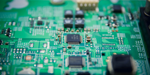
Vias are useful for high-density PCBs where all connections cannot be placed on one layer. In short, vias are barrel-shaped vertical conductive holes that help make connections between multiple layers of the PCB.
Blind and Buried Vias
These two vias are popular when you need to make connections between multiple layers of blind and buried vias in a printed circuit board.
Simply put, blind vias connect the outermost layer of the board to one or more inner layers, but do not run through the entire PCB. Blind vias free up space for fine pitch BGA components. Since vias terminate in the last connection layer, they also help reduce signal stubs during drilling.
Buried vias, on the other hand, connect two or more inner layers, but do not penetrate to the outer layers. As their name implies, they hide beneath layers and free up surface space without affecting traces or surface components on the top or bottom layers.

Both blind and buried vias have huge uses in high density interconnect PCBs. Such PCBs offer several advantages, including but not limited to: high layer density, better power delivery, the ability to use smaller pitch devices
Types of blind holes
There are roughly three types of blind vias
Sequential lamination of blind vias.
Controlled depth blind vias.
Laser drilling blind holes.
This is produced by laminating a sheet of photosensitive resin to the core. The layer of photosensitive material is covered with a pattern covering the areas where the holes are to be created. It is then exposed to light, which causes the material on the PCB to harden. After that, the PCB is immersed in the etching solution. After the etching process, copper is plated in the holes and on the outer surface. These vias are often used to create BGA packages.
Sequential Lamination Blind Vias
This is created by processing a thin sheet of laminate. The laminate is drilled, plated and etched. The other side is left as a solid copper sheet. The subassembly is then laminated. Handles combinatorial lamination to create the outer layers of a multi-layer PCB. This process requires some extra steps, so the price of such vias is high. In addition, handling thin laminates also results in yield losses.

Controlled depth drilling blind holes
These are created like vias. A drill can only penetrate the PCB in a certain way. Be careful to see that none of the features below the drilled hole are in contact with the drilled hole. Plating copper in drilled and through holes. These vias are the cheapest. However, they have a limitation that the holes must be large enough for a mechanical drill to create them, and the area below them must remain free of circuits.
Laser drilling blind holes
These are created after all layers in the PCB are laminated and before the outer layers are plated and etched. The copper on the outer layer is ablated by using a CO₂ laser or an Eximer laser.
CO₂ lasers are very powerful and can drill holes quickly. However, with this laser, the drilling step must be preceded by an etching step. Excimer lasers can drill through copper balances in PCBs and the underlying dielectric material to form blind vias.
Advantages of blind vias
Blind vias help reduce parasitic capacitance. This is achieved by shortening the length of the through holes and reducing their diameter. Therefore, blind vias are a good way to connect signal lines operating above 4.8 Gb/s.
Some limitations of blind vias include:
Blind vias are blind holes in a PCB, to ensure proper plating, the diameter of the hole should be equal to its depth. This requires an aspect ratio of 1:1 or less. Some manufacturers require the diameter to be 1.5 times the depth.
Drilling with blind holes requires stopping at a predetermined level. With a laser drill, although the drill needs to go through the copper on layer 1, it should not drill the copper connection pads on layer 2. This requires careful calibration.
Another issue has to do with soldering components to pads where blind vias are placed. When solder paste is applied to the pads, air in the blind vias is trapped under the holes that cannot weaken the joint.
Aspects to keep in mind when making vias:
Vias can be made before or after multilayer lamination. One or more cores are drilled and plated through holes. Then build and push the stack.
When creating blind holes, it is important to know the drilling depth. If the hole is too deep, it will affect signal integrity, and if the hole is too shallow, the connection will be incorrect.
It's also important to plug the via with metal or thermal/electric epoxy and plated it with copper. Otherwise, the air bubbles will move up and affect the solder joint.
Another aspect to keep in mind is that vias must go through an even number of copper layers. In addition, if the via is completely enclosed within the termination point, it will result in a significant increase in cost.
When discussing blind and buried vias, it is also important to understand what stacking and microvias are:
Stacked vias further help improve PCB size and density considerations. Therefore, it greatly contributes to miniaturization and high signal transmission speed.
Stacked vias are required if you have blind vias with aspect ratios greater than 1:1, or if your drill holes need to span multiple layers. These are laminated blind or buried vias. Stacked vias not only save space and help achieve high density, but also provide greater flexibility when it comes to internal connections, as well as better routing capabilities and less parasitic capacitance.
Microvias are small vias that provide more routing space on a circuit board and reduce parasitic capacitance. However, such through holes require more drilling time.
It is important to choose the right electronics contract manufacturing partner with the necessary experience with blind and buried vias.
KFPCBA as a one-stop PCBA manufacturing service provider, we use advanced methods and technologies to provide you with the best PCB manufacturing services, our delivery capabilities, unparalleled quality and customer service make us stand out.
Comment on this article here
-
No comment

Ripple
Hi everyone, I'm Ripple, Sales Director of KFPCBA Tech Ltd. If you are looking for a one-stop PCB and PCB assembly manufacturer in China, KFPCBA is your best choice! Please feel free to contact our team! Thanks!
Contact me now


