


 tel:+86-18825224069
 email:
 address:201, Factory 6, Longhui Industrial Park, Fuqiao 3rd District, Xinhe Community, Fuhai Street, Baoan District, Shenzhen china
Multi-layer How PCB Board is Made: Comprehensive Guide to Manufacturing
Release date:2023-05-25 11:29:57 Number of views:0
The evolution of electronic devices has necessitated the use of printed circuit boards (PCBs) with multiple layers of copper tracks and components. Multi-layer PCBs are now a crucial component of electronic engineering, used in various devices ranging from mobile phones to computers to anything that requires intricate electronic circuitries. In this comprehensive guide, we will delve into the nitty-gritty of how multi-layer PCBs are made, including the materials, manufacturing processes involved, and the design considerations. Whether you are an engineer, a student, or simply someone curious about how technology works, this article will offer valuable insights into the fascinating world of electronics manufacturing.

Design and Prototyping:
The first step in manufacturing a multi-layer PCB board involves designing the circuit layout using specialized software. Engineers carefully plan the component placement, signal traces, and power distribution. Once the design is finalized, a prototype is created to test and verify the functionality of the circuit.
Material Selection:
The choice of materials for a multi-layer PCB board is critical. The base material, commonly referred to as the substrate, is typically made of fiberglass-reinforced epoxy laminate known as FR-4. Copper foil is laminated to both sides of the substrate to provide electrical conductivity. The thickness and type of copper foil are chosen based on the specific requirements of the circuit.
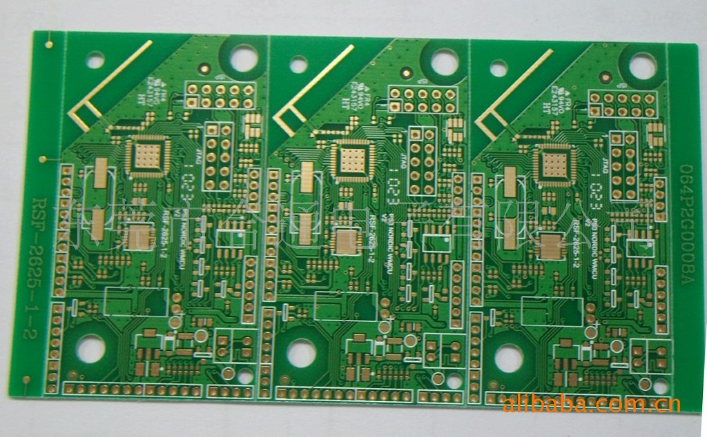
Inner Layer Processing:
In this step, the inner layers of the multi-layer PCB board are fabricated. The substrate material is coated with a photosensitive material known as a resist. The circuit pattern is then transferred onto the resist using a photographic process. The exposed areas are etched away, leaving behind the copper traces that form the circuitry. Multiple inner layers are produced in this manner.
Layer Alignment and Bonding:
After the inner layers are ready, they are aligned and bonded together. An insulating layer called the prepreg, which consists of epoxy resin and glass fibers, is placed between the inner layers. This stack-up is subjected to heat and pressure, which causes the prepreg to melt and bond the layers together, forming a solid multi-layer structure.
Drilling:
Precise holes, called vias, are drilled through the entire stack of layers. These vias act as electrical connections between the different layers of the PCB. The drilling process is computer-controlled to ensure accuracy, and the holes are coated with a conductive material to establish electrical continuity.
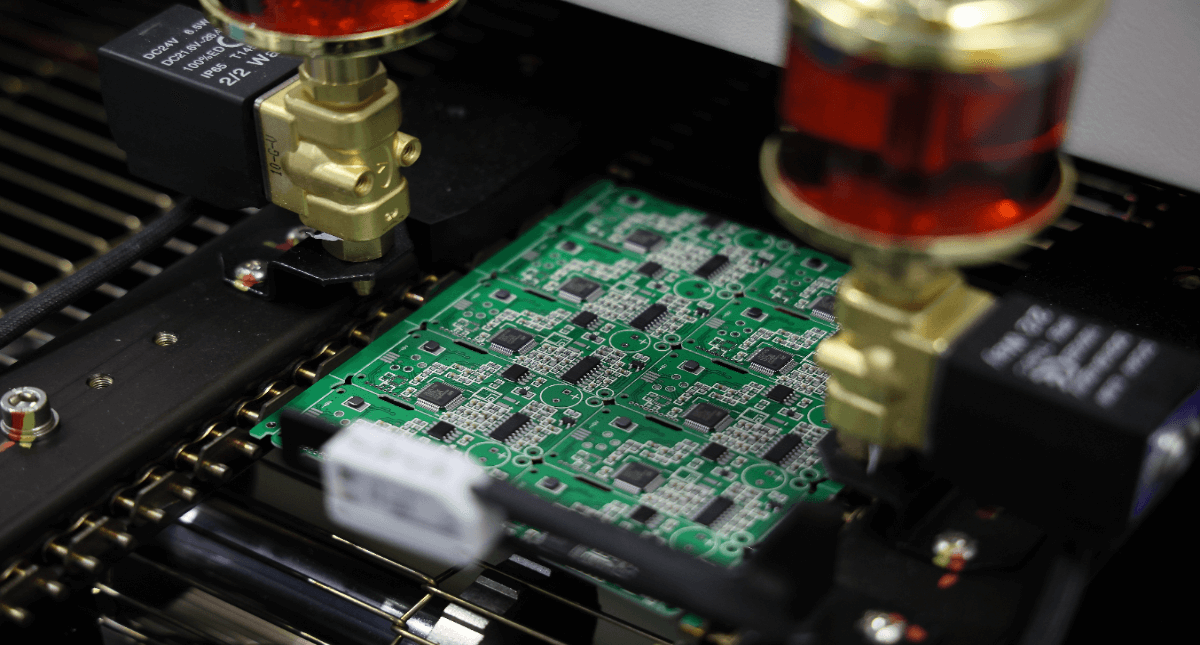
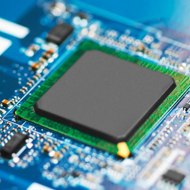
Plating and Surface Finishing:
The drilled vias and the exposed copper traces on the outer layers are plated with a thin layer of copper to enhance conductivity. The excess copper is then removed, leaving behind the desired circuit pattern. Next, a protective solder mask is applied to the surface, providing insulation and preventing unintended electrical connections. Lastly, a layer of metallic finish, such as gold or tin, is applied to protect the exposed copper and enhance solderability.
Testing and Quality Assurance:
To ensure the reliability and functionality of the multi-layer PCB board, rigorous testing is conducted. Various techniques, including automated optical inspection (AOI) and electrical tests, are performed to detect any defects or faults in the circuitry. This step helps identify and rectify any issues before the board is ready for assembly.
Conclusion:
The manufacturing process of multi-layer PCB boards is a complex and precise undertaking. Each step, from design and prototyping to drilling and surface finishing, requires meticulous attention to detail. By understanding the intricacies of this process, we can appreciate the remarkable engineering behind the multi-layer PCB boards that power our modern electronic devices.
Comment on this article here
-
No comment

Ripple
Hi everyone, I'm Ripple, Sales Director of KFPCBA Tech Ltd. If you are looking for a one-stop PCB and PCB assembly manufacturer in China, KFPCBA is your best choice! Please feel free to contact our team! Thanks!
Contact me now
Relevant content you may be interested in
Related articles


