


 tel:+86-18825224069
 email:
 address:201, Factory 6, Longhui Industrial Park, Fuqiao 3rd District, Xinhe Community, Fuhai Street, Baoan District, Shenzhen china
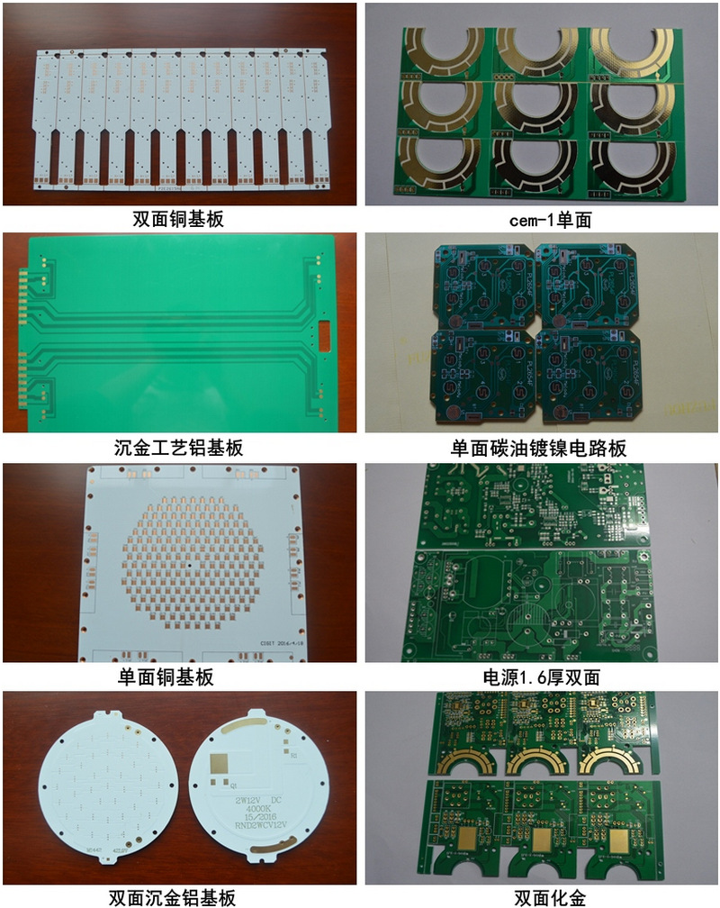
PCB/PCBA Prohibited Design And Prohibited Installation Process (72 Items)
Release date:2022-11-23 16:13:32 Number of views:96
PCB/PCBA prohibited design and prohibited installation process (72 items)
PCB/PCBA prohibited design and prohibited installation process (72 items)
Asymmetrical pad ends are prohibited.
Except for high-frequency microwave circuit boards , it is forbidden for any components and wires to share pads.
It is forbidden to overlap the design of wires and component pads.
It is forbidden to silk screen design on the pad.
It is forbidden to design silk screen on the large-area soldering surface.
It is forbidden to arrange components within 5mm of the process edge, clamping edge or printed board edge.
Printed circuit board assemblies are not allowed to have jumpers.
It is forbidden to forcibly install discrete components when the pin spacing is inconsistent with the corresponding hole spacing designed on the PCB.
Via holes and vias are not allowed in the pad.
Vias and vias are not allowed on the bottom of the component.
The spacing between solder ends of components, and the distance between solder ends and component bodies is not allowed to violate the minimum electrical clearance requirements.
No bridging or stitching of components is permitted.
Hard mounting on the PCB is not allowed.
It is not allowed to mount components to form an airtight installation.
Components such as power transistors, rectifier diodes, relays, power modules, pins, and electrical connectors, and thick leads with a diameter of ≥1.3mm are not allowed to be directly welded to PCB pads to form hard connections.
It is not allowed to install by extending the leads of components.
The distance from the components on the printed circuit board to the edge of the printed circuit board shall not be less than 1.6mm.
Vertical mounting of surface mount components is not allowed.
Except for high-frequency microwave circuit boards, mounting and welding of plug-in components is not allowed.
Plug-in components are not allowed to be installed vertically.
Except for high-frequency microwave circuit boards, it is forbidden for component leads to overlap other component leads or pads.
It is forbidden for wires to share a metallized hole with other component pins.
It is forbidden for component leads to share a metallized hole.
It is forbidden to use component welding terminals as connection points or via holes as connection points.
It is forbidden to design component pads directly in the grounding area.
Mounting of radial components on board is prohibited.
It is forbidden to install and solder moisture-sensitive components directly without baking and dehumidification treatment.
It is forbidden to plug non-board-mounted leaded components into single-side pads of metallized holes.
Do not use solder mask as an insulating layer.
It is forbidden to design that the gap between the component pin and the metallized hole exceeds 0.2mm~0.4mm; it is forbidden to use the method of expanding the hole or reducing the size of the pin to meet the requirements of the gap.
The thickness of the gold-plated layer on the surface of the printed circuit board pad shall not exceed 0.45mm.
OSP and electroplating nickel-gold processes should not be selected for the solderability plating on the surface of printed circuit boards.
Vias are prohibited as mounting holes for fasteners.
It is not allowed that the seat pad for component installation is not in contact with the board surface or tilted, and the seat pad is reversed to block the metallization hole.
Terminals and rivets should not be used for interface or interlayer connections. Metallized holes that serve as interface connections cannot be used to mount components.
Blind rivets are prohibited for electrical connections.
It is forbidden to install components in metallized holes (via holes) that serve as interface connections.
It is forbidden to hard-connect the leads of components with a diameter ≥ 1.3mm directly on the pad.
It is forbidden to insert more than one wire or component lead into any printed board mounting hole.
Components shall be mounted without impeding solder flow to the pad on the top side of the metallized hole.
Except for high-frequency circuits, it is not allowed to overlap other components on the printed wires.
It is not allowed to overlap other components on the component leads.
It is not allowed to install by extending the leads of components.
The distance from the components on the printed circuit board to the edge of the printed circuit board should not be less than 1.6mm.
When the diameter of the metallized hole is smaller than the outer diameter of the component lead, any form of hole expansion is prohibited.
Reverse assembly is strictly prohibited when flat-package integrated circuits are assembled.
Components should be in the middle of the two pads on the circuit board. Chip components should not overlap or be placed sideways, nor should they bridge the gaps of other components (such as wire leads or other properly installed devices).
Printed circuit board assemblies with a warpage greater than 0.5% are strictly prohibited from correcting or anti-deformation installation.
It is forbidden to hard-connect the F-type package power device directly to the solder joint.
Do not allow insulated wires to touch directly over solder joints, fasteners, or the pads of any test points.
It is forbidden to lay and glue the wires (wire harness) on the components.
Except for microwave circuits, it is forbidden to install single-sided lead devices (such as TO packaged transistors, metal packaged relays, filters, crystal oscillators, etc.) without insulation isolation design.
It is forbidden to apply insulating materials such as conductive silicone grease on the contact surface that requires contact resistance.
It is forbidden to manually solder surface mount chip ceramic capacitors without preheating and directly soldering.
Hammering (including rubber hammers) is prohibited on products incorporating printed circuit board assemblies.
Vertical installation of axial components is prohibited.
When microwave devices such as radio frequency electrical connectors are soldered in parallel with the microstrip circuit board, the gap with the microstrip line is not allowed to exceed the range of 0.2mm~0.05mm.
It is not allowed to fill the gap larger than 0.2mm for welding.
The inner conductor of the active RF electrical connector is not allowed to be directly soldered on the microstrip circuit board.
It is not allowed to weld the pin welding end of the radio frequency electrical connector and the microstrip line on the microstrip circuit board for vertical hard installation.
Ultrasonic cleaning is not permitted for printed board assemblies.
Do not use Freon (F113) as cleaning fluid.
Saponified cleaning agents are forbidden to be used on PCBA with aluminum components.
It is forbidden to use printed circuit board components and cable solder joints without cleaning.
Except for radio frequency circuit boards and microwave circuit boards, it is forbidden to install and use any printed circuit board components without three-proof treatment.
Except for radio frequency circuit boards and microwave circuit boards, any printed circuit board assembly is prohibited from undergoing three-proof treatment if the cleanliness does not meet the relevant standards.
Adhesives that damage components and assemblies are prohibited.
Prohibit the use of potting materials that have a corrosive effect on the assembly;
Potting and bonding are not allowed for wirewound resistors with a power consumption of 1W or more.

It is forbidden to use only silicone rubber to fix the wire harness with a diameter greater than 8mm.
Coils with magnetic cores (more than 3.5g in weight), transformers and other devices that do not support lead wires are prohibited to be glued only with silicone rubber.
It is forbidden to install the crystal sideways and only use silicone rubber to fix it.
2 Disabled Design and Disabled Installation Process of Cable Assemblies (62 items)
(1) Wire end treatment
It is forbidden for wires (including multi-strand wires) to adapt to the hole diameter of the pad or the inner diameter of the solder cup by mechanically trimming or cutting off part of the core wire to reduce the number of strands to reduce the diameter before welding.
It is forbidden to have visually visible circumferential (transverse) scratches on the surface of single-strand leads and component pins (such as circumferential cuts on inner conductors caused by semi-rigid cable stripping, circumferential grinding or scraping for enameled wires) removal of circumferential cuts).
It is forbidden to form multi-strand wires with tinning first.
It is forbidden to use sharp tools such as scrapers to remove oxides on the surface of component leads.
It is forbidden for the solder to penetrate into the insulation layer of the wire and extend to the part where the wire needs to remain insulated during tinning.
It is forbidden to weld the gold-plated wire core wires, component leads/solder ends, and the diameter of the welding parts of various terminals that have not been treated with gold and tin.
Tin enamelling of stranded conductors for crimp connections is prohibited.
Tin-coating of stranded conductors for threaded fastener connections is prohibited.
Tin-coating of multi-strand wires used for mesh connections is prohibited.
It is forbidden to use tinning treatment for multi-strand wires used in heat shrinkable welding devices.
Do not use chemical strippers on stranded wire.
(2) RF cable
It is strictly forbidden to forcibly assemble and weld when the RF cable does not match the RF connector.
During the assembly and welding process of the RF circuit, it is strictly forbidden to install and weld the insulation cuts in the circuit unevenly.
Diametrically crimping the outer cable sheath should not be used as the primary means of cable retention.
It is strictly forbidden to bend the RF cable with a radius smaller than that specified in the product manual.
When disassembling the RF cable assembly, it is strictly forbidden to remove the RF cable assembly by pulling and twisting the RF circuit, so as to ensure that the connector and cable at the end of the cable do not rotate.
It is strictly forbidden for SFT semi-rigid cables to be assembled and welded without baking pretreatment according to regulations.
(3) Transition of wire and cable
Conductor cable transitions must not be used to extend the cable harness.
Conductor cable transitions are prohibited within the cable harness.
Short-term connection is not allowed.
Any wires are not allowed to be used continuously.
Special adapter accessories must be used for wire transfer, and the use of: a) lap welding of wire core wires; b) wrapping welding of wire core wires; c) hook welding of wire core wires; d) plug welding of wire core wires. The four methods are not allowed even if they are protected with heat shrinkable sleeves after welding.
(4) Wire crimping
Single stranded wire should generally not be used in pre-insulated barrels for compression-resistant crimps and molded-in crimps.
Crimp connections are generally not allowed to use single-strand wires.
Crimp connections are generally not allowed to use tinned core wire.
In any case, crimping should be completed in one full crimping cycle, repeated crimping should be avoided, and overlapping indentations are not allowed.
It is strictly forbidden to straighten crimped connectors that are bent and deformed by crimping.
The method of folding the wire core should not be used to increase the cross-sectional area of the wire to accommodate the larger crimping barrel.
It should not be used to reduce the cross-sectional area of the wire by leaving some wire cores outside the crimping barrel or trimming the wire core to accommodate the smaller crimping barrel.
All wire cores of the wire should be neatly inserted into the crimping barrel without any bending.
The safe current carrying capacity of the crimped wire on each contact shall not be greater than the maximum operating current allowed by the connected connector contacts.
The outer diameter of the wire passing through the sealing ring must not exceed the hole diameter on the sealing ring, and the sealing ring must not be twisted and deformed.
It is not allowed that the wire is not inserted to the bottom and the observation hole of the contact couple has only part of the core wire.
It is not allowed that the wire is not inserted to the bottom and there is no core wire in the observation hole of the contact couple,
The wire entry edge of the contact couple must not be deformed by crimping.
Indentations are not permitted outside the crimp area.
Crimps are not allowed to deform the inspection window.
Cracks and cracks are not allowed to be seen on the contact couple.
It is not permissible that the conductors have been kneaded together prior to insertion into the connector.
For any reason, if the tool's calibration equipment is damaged, it must be immediately evacuated from the workplace and recalibrated ; any definite or suspected failure of the crimping tool must be immediately evacuated from the workplace and recalibrated; crimping Any confirmed or suspected tool failure must be immediately removed from the workplace and recalibrated.
(5) The whole machine and cables
When the wire is in the welding groove of the electrical connector, on the lead of the panel component, or on the printed board, hard bending is not allowed at the root of the wire, and there must be a suitable arc for stress relief, and a margin of 2 to 3 times of welding must be left .
The safety gap between the wire and the fastening is prohibited to be less than 5mm or laid from above the fastening.
It is forbidden for wires to pass through the inner layer of component leads or under the cloud device body. It cannot be laid or routed on the components.
It is forbidden for the insulating layer of the wire bundle to come into contact with the edges, bumps, metal components and solder joints of metal parts.
It is forbidden to directly contact the insulation layer of 100V and above high-voltage wires with metal parts.
Except for direct grounding requirements, direct contact between metal shells and other fasteners and metal parts is prohibited.
It is forbidden to lay or route wires on the through-hole solder joints.
It is forbidden to lay wires vertically close to the leads of relays, high-power tubes, etc. when the safety gap is less than 5mm.
Do not route or route wires through through-holes without protection.
It is forbidden to lay wires and wire bundles in the air and route them inside the chassis.
It is strictly forbidden to connect the grounding wire of the external cable shield to the soldering part of the connector.
It is forbidden to install two or more wires in one metallized hole.
The laying distance of the wire harness on the PCBA should not be less than 5mm.
Interpenetration and crossover of wires are not allowed between printed circuit board components and panel components.
It is forbidden to overwhelm the root of the wire for assembly and welding.
It is forbidden to fix the wiring harness to the main ground in the chassis.
It is forbidden to install and weld with components suspended in the air with one arm.
It is forbidden to weld the PTFE wire without fixing it.
The lead wires or wires of components on the printed circuit board should be fixed on the lead holes or terminals, and must not be overlapped with other lead wires or wires. A lead hole can only fix one lead wire or wire.
The bending part of the cable should be no less than 30mm away from the tail cover opening or the back edge of the shielding layer. In the cable manufacturing, laying and electrical connector plugging and unplugging operations , it is forbidden to bend the cable bundle within the 30mm "forbidden zone". .
There should be no interpenetration and crossover of wires between the diameter of each PCBA and the panel components.
The wire bundle should not be placed next to the relay pin leads or perpendicular to the pin leads or by itself.
Comment on this article here
-
No comment

Ripple
Hi everyone, I'm Ripple, Sales Director of KFPCBA Tech Ltd. If you are looking for a one-stop PCB and PCB assembly manufacturer in China, KFPCBA is your best choice! Please feel free to contact our team! Thanks!
Contact me now


