


 tel:+86-18825224069
 email:
 address:201, Factory 6, Longhui Industrial Park, Fuqiao 3rd District, Xinhe Community, Fuhai Street, Baoan District, Shenzhen china
Guide to PCB Manufacturing: From Design to Production
Release date:2023-04-13 14:17:49 Number of views:0
The process of designing and manufacturing printed circuit boards (PCBs) can be complex and time-consuming, but it's a crucial step in building electronic devices. PCBs are essential components of modern electronics, providing connections between electronic components and controlling the flow of electricity. To ensure that a PCB functions correctly, it’s important to understand the steps involved in its design and production. In this blog, we'll provide a comprehensive guide to PCB manufacturing, covering everything from the initial design phase to the final production of a high-quality PCB. So, whether you're a professional electronics engineer or a hobbyist looking to build your own electronic devices, this guide will take you through the essential steps of PCB manufacturing.

Section 1: Understanding PCB Design
PCB design is a critical first step in the manufacturing process. It involves creating a schematic diagram that outlines the components and layout of the circuitry. PCB design software and tools are commonly used to create these diagrams. In addition, there are different types of PCBs depending on the application, size, and complexity of the device.
The design process requires a thorough understanding of the components, their specifications, and their interactions. This requires collaboration between the engineers and designers, and the use of clear documentation and communication. Once the design is complete, it’s important to review it multiple times to ensure accuracy and avoid errors.
Section 2: PCB Layout and Component Placement
After the schematic diagram is complete, the next step is to create the PCB layout (also known as the board’s topology or geometry). This includes placement of the components, traces, and vias. The layout is crucial as it affects the signal integrity, electrical performance, and manufacturability of the PCB.
Guidelines for PCB layout should be followed, such as minimum clearance and trace widths, and keeping components grouped based on function. There are also considerations for component placement, such as avoiding thermal hotspots, minimizing signal loop areas, and ensuring accessibility for testing and troubleshooting. The factors affecting component placement can be numerous, including size and shape of the device, power requirements, and environmental factors.

Section 3: PCB Fabrication Process
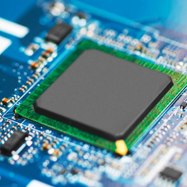
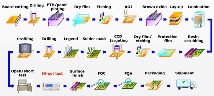
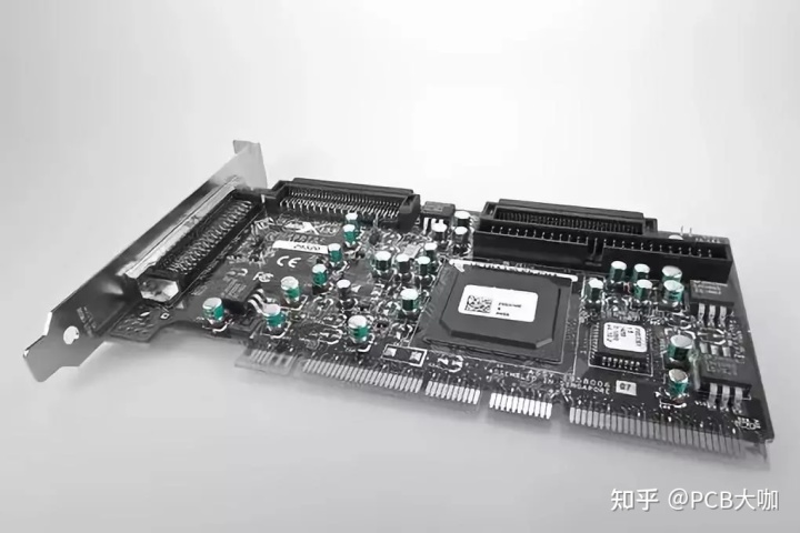
Once the layout is complete, and the design is finalized, it’s sent off for fabrication. PCB fabrication involves several steps, PCB manufacturing process including imaging, drilling, plating, and etching. This results in the creation of the copper traces and pads that make up the electrical connections.
The materials used for PCB fabrication can vary, depending on the complexity of the design and the specific requirements of the application. Common materials include copper, laminates, and solder masks. PCB fabrication techniques include both additive and subtractive methods, depending on the type of board and the complexity of the design.

Section 4: PCB Assembly and Soldering
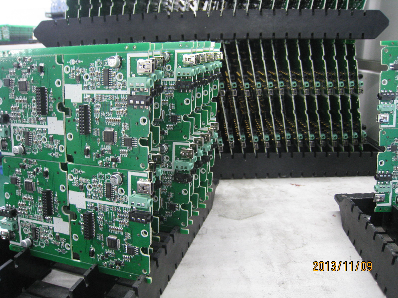
After the PCB is fabricated, the components are added through the process of assembly. This typically involves surface-mount technology (SMT) and through-hole technology (THT), which offer different advantages and disadvantages depending on the specific components and application.
Soldering is a critical part of PCB assembly, and there are various techniques used to ensure high-quality connections. Some of these techniques include wave soldering, reflow soldering, and hand soldering. However, the process of soldering can also introduce potential issues, such as poor connections, short-circuits, or overheating. These common soldering issues can be solved through troubleshooting and repair.

Section 5: PCB Testing and Quality Control
To ensure high-quality PCBs, testing and quality control measures are put in place. This includes both functional and performance testing, as well as visual inspections and checks for any manufacturing deficiencies.
There are different types of testing that can be performed, including continuity testing, in-circuit testing, and functional testing. Quality control measures may include statistical process control, incoming material inspections, and audits. Additionally, there are common faults that may be encountered during testing or after deployment, such as open or short circuits, or solder defects.
Section 6: Advanced PCB Manufacturing Techniques
There are several advanced techniques in modern PCB manufacturing that go beyond the traditional methods. These advanced PCB manufacturing techniques include high-density interconnect (HDI) PCBs, microvia PCBs, and flex circuit PCBs.
HDI PCBs have higher component density and smaller traces, allowing for more functionality in a smaller space. Microvia PCBs use vias smaller than 0.15mm, resulting in smoother surfaces and better signal integrity. Flex circuit PCBs are designed to accommodate the device’s movement and flexibility, making them ideal for applications where space is limited.
Section 7: Choosing the Right PCB Manufacturer
Choosing a PCB manufacturer requires careful consideration of the many factors involved. This includes considering the manufacturer’s experience and expertise, their facility, and equipment, the range of services they offer, and their quality control and testing procedures.
When selecting a PCB manufacturer, it’s also important to ask the right questions and avoid common mistakes. Some important questions to ask include how long they’ve been in business, what certifications they have, and what their turnaround times are. Common mistakes to avoid include not reviewing initial quotes thoroughly, not providing complete documentation, and not communicating effectively with the manufacturer.

Section 8: Conclusion
PCB manufacturing is a complex process that requires careful planning, clear communication, and the use of the right tools and techniques. By understanding the key steps involved, from design to production, electronics professionals and hobbyists alike can ensure that their PCBs are of the highest quality and function correctly.
As modern electronics continue to evolve, there will likely be new advancements and innovations in PCB manufacturing. However, the importance of quality control, testing, and collaboration between engineers, designers, and manufacturers will remain critical in the development of electronic devices.
Comment on this article here
-
No comment

Ripple
Hi everyone, I'm Ripple, Sales Director of KFPCBA Tech Ltd. If you are looking for a one-stop PCB and PCB assembly manufacturer in China, KFPCBA is your best choice! Please feel free to contact our team! Thanks!
Contact me now
Relevant content you may be interested in
Related articles


