


 tel:+86-18825224069
 email:
 address:201, Factory 6, Longhui Industrial Park, Fuqiao 3rd District, Xinhe Community, Fuhai Street, Baoan District, Shenzhen china
The layout of PCB board DSP and the placement of components shall be noted
Release date:2022-11-09 17:19:25 Number of views:0
The layout of PCB board DSP and the placement of components shall be noted
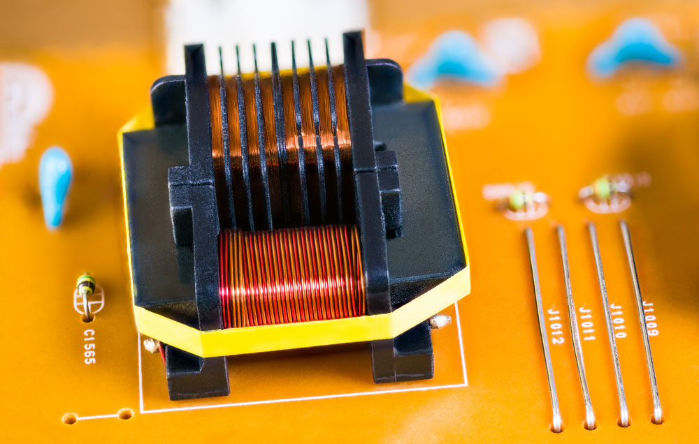
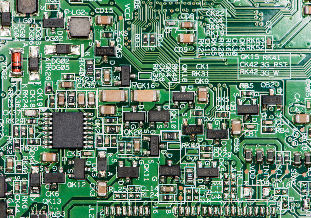
In order to get the best performance of DSP System, the Layout of components is very important. DSP, Flash, SRAM and CPLD devICes shall be placed first, and cabling space shall be carefully considered, then other ICs shall be placed according to the principle of functional independence, and finally I/O port shall be placed. Considering the size of PCB based on the above layout: if the size is too large, the printed line will be too long, the impedance will increase, the anti noise ability will decline, and the cost of board making will also increase; If the PCB is too small, the heat dissipation is poor, and the space is limited, and adjacent lines are vulnerable to interference. Therefore, components shall be selected according to actual needs, and PCB size shall be generally calculated in combination with wiring space. When laying out the DSP system, pay special attention to the placement of the following devices.
(1) High speed signal is laid out in the whole DSP system. DSP, Flash and SRAM are the main high-speed digital signal lines. Therefore, the distance between devices should be as close as possible, and their connecting lines should be as short as possible and connected directly. Therefore, in order to reduce the impact of transmission lines on signal quality, high-speed signal routing should be as short as possible. Also consider that many DSP chips with speeds up to hundreds of MHz need to do snake winding. This will be highlighted in the cabling below.

(2) The layout of digital analog devices in DSP systems is not a single functional circuit, and a large number of CM0S digital devices and digital analog hybrid devices are used, so digital/analog devices should be separated. The analog signal devices shall be concentrated as much as possible, so that the analog ground can draw an independent area belonging to the analog signal in the middle of the whole digital ground to avoid the interference of the digital signal to the analog signal. For some digital analog hybrid devices, such as D/A converter, it is traditionally regarded as an analog device, which is placed on the analog ground and provided with a digital loop, so that the digital noise can be fed back to the signal source to reduce the impact of digital noise on the analog ground.
(3) The clock layout shall be far away from I/O line and connector as far as possible for clock, Chip selection and bus signal. The clock input of DSP system is easy to be disturbed, so its processing is very important. Always ensure that the clock generator is as close to the DSP chip as possible and that the clock line is as short as possible. The case of the clock crystal oscillator should preferably be grounded.
(4) Decoupling layout In order to reduce the voltage transient overshoot on the IC chip power supply, a decoupling capacitor is added to the IC chip, which can effectively remove the impact of burrs on the power supply and reduce the power loop reflection on the PCB. Adding decoupling capacitors can bypass the high-frequency noise of integrated circuit devices, and can also be used as energy storage capacitors to provide and absorb the charging and discharging energy at the moment of opening and closing the doors of integrated circuits.
PCB manufacturers, PCB designers and PCBA manufacturers explain the layout of PCB board DSP, and pay attention to the placement of components.
Comment on this article here
-
No comment

Ripple
Hi everyone, I'm Ripple, Sales Director of KFPCBA Tech Ltd. If you are looking for a one-stop PCB and PCB assembly manufacturer in China, KFPCBA is your best choice! Please feel free to contact our team! Thanks!
Contact me now
Relevant content you may be interested in
Related articles


