


 tel:+86-18825224069
 email:
 address:201, Factory 6, Longhui Industrial Park, Fuqiao 3rd District, Xinhe Community, Fuhai Street, Baoan District, Shenzhen china
Bare Printed Circuit Boards: All About Blank Boards
Release date:2022-11-03 17:29:50 Number of views:0
Assembling PCB with hundreds of components can be an expensive and complex process that consumes a lot of time. Therefore, it is necessary to ensure the underlying printed wiring board functions optimally before assembly to avoid costly board-level repair. Bare printed circuit board gives you a blank platform that you can test before assembly to avoid these expensive repairs. We will look at these PCBs to analyze their benefits from an electronics production standpoint. Let's get right into it!
What is a Bare Printed Circuit Board?
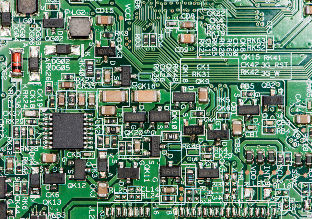
In a nutshell, a bare PCB board is a circuit board without thru-holes or electronic components. It is the skeleton of conventional PCBs and consists of a substrate, conductive pathways, metal coating, and patterns.
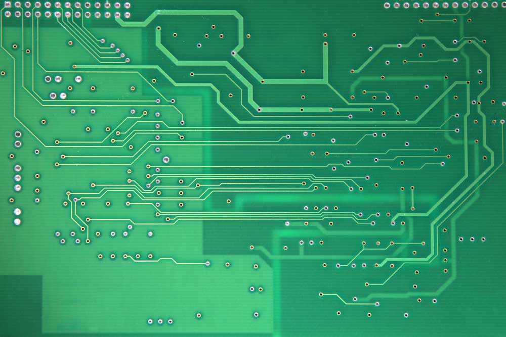
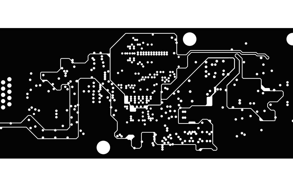
A bare-printed circuit board
Some industry experts refer to bare boards as PCBs or blank PCBs, while assembled boards are PCBA.
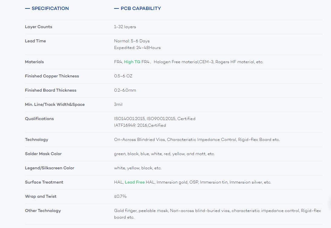
Bare Printed Circuit Board Capabilities
Why Use a Bare Board?
A bare board is like a skeleton or backbone that forms a frame for customized configuration. Therefore, you can use it to test designs, functionality, and concepts before assembling expensive components.
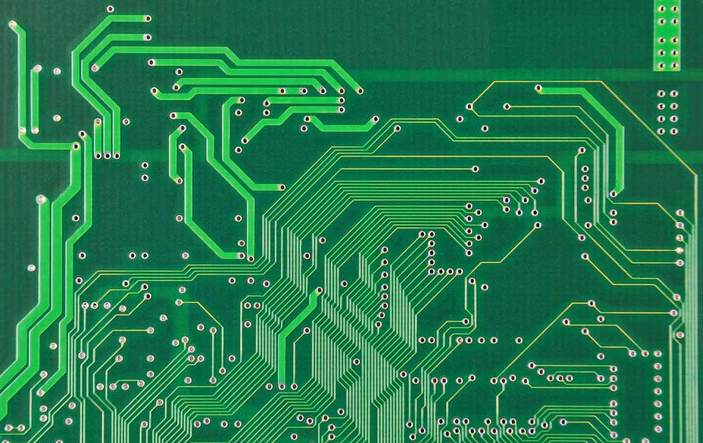
A bare PCB
The testing process helps eliminate issues that can affect the usability of an electronic device. On top of that, the bare board provides mechanical support to the circuit and electrical components.
Advantages of Bare Boards
Besides mechanical support and creating a compact circuit for testing, bare boards have the following advantages.
Early Defect Detection
The bare board's surface does not have electronic parts or other obstructions. So you can examine their design and structure to detect any issues with select single components or copper patterns. It will be cheaper to rectify these issues at this stage than if you encounter them after assembly.
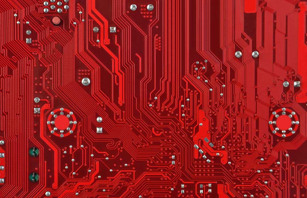
A red-printed circuit board with no components
Saves Time
Early electrical testing and prototyping ensure you achieve design-specific functionality. So you won't waste time assembling functional components on a faulty PCB.
Cost Saving
Since bare board testing is a foundational process that helps with board design, fabrication, and testing, it ensures the PCB is durable and functional. Early problem detection is cheaper to fix, so you will minimize losses and possibly avoid damaging expensive components by soldering them to a faulty board. Also, time is money. So saving time implies you save money.
Bare Board Manufacturing Process
Fabricating bare boards pcb involves the following steps.
Pre-Production
After sending the Gerber design/board layout file to the manufacturer with the production and customization information, the engineers align the specifications and capabilities to ensure compliance.
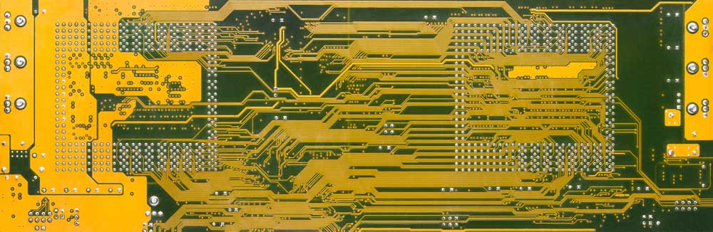
A Gerber file showing the layout of a PCB’s inner layers
Inner-Layer Imaging
A focused laser beam defines the PCB traces into the board directly.
Inner Layer Etching
The etching process removes all excess copper residue from the PCB to ensure the circuitry/copper pattern matches the design.
Lamination
Oxide layers are the most typical printed circuit board laminates. So lamination involves applying an oxide layer to the inner board layer, then stacking them together. The oxide layer acts as insulation in multilayer boards. A copper foil also gets added. But the inner layers require a complete machine inspection before lamination to avoid mistakes.
PCB Drilling
Drilling creates holes that act as electrical connection contacts and optimize layer links.
Electroless Copper Deposition
The next step is electroless copper deposition, which deposits a thin copper layer into the drilled holes. This process conceals the holes and seals the board.
Outer Layer Imaging
This imaging process removes the dry film to ensure the circuit runs as required. After that, additional copper gets plated.
Graphic Plating
This plating process places an extra layer on the dry film parts. After copper deposition, the additional tin plating prevents oxidation for maximum durability.
Outer Layer Etching
Outer layer etching removes the excess copper residue and dry blue film. The tin-metallic plating safeguards the essential copper circuitry components.
Solder Mask Curing
Some sections of the PCB get exposed to UV light, while others get removed. After that, the board undergoes a curing process using a solder mask, which creates a smooth, high-quality finish.
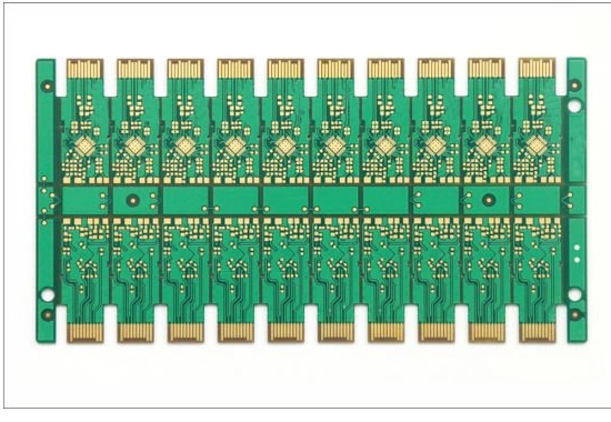
A multilayer PCB with green solder stop mask
Surface Finishing
Surface finishing creates organic or metallic solderable surfaces for surface-mount component placement and soldering.
Electrical Board Testing
The board is complete at this point, and the next step is to test if the PCB traces are functional and conduct electric signals as required. You can test the boards using fixture-less testing, flying probe, or universal grid testing.
V-Scoring and Profiting
Production panels get routed into specific shapes and sizes to match the production file. V-scoring involves cutting V grooves on the board's top and bottom for easy layer or component-level separation without damage.
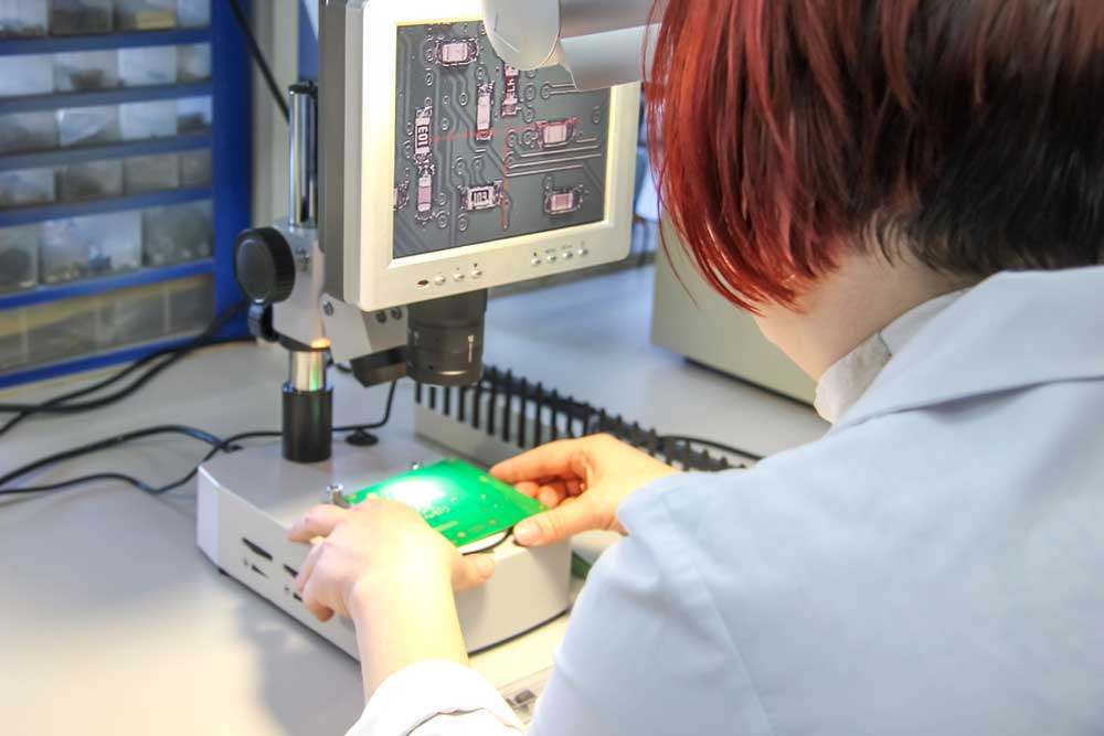
Visual Inspection
The final step is an optical inspection of the entire board by a team of skilled and qualified engineers who check if the board meets the required standards. Once the boards pass the inspection process, they go into packaging and delivery.
An engineer is inspecting a PCB visually.
What is Bare PCB Testing?
Bare board testing is the electrical testing done on blank PCBs to evaluate the isolation and continuity of the wiring board connections. Isolation testing checks the resistance between two electrical connections, while continuity testing ensures the circuits don't have open points that can impede current flow.
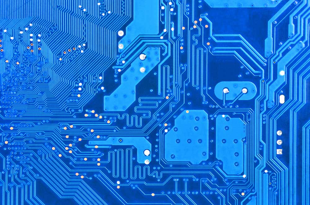
A blue-printed circuit board
Types of Bare Board Testing
The traditional method of testing bare boards is by using a digital multimeter. But the process is not feasible with modern multilayer boards because they are complex.
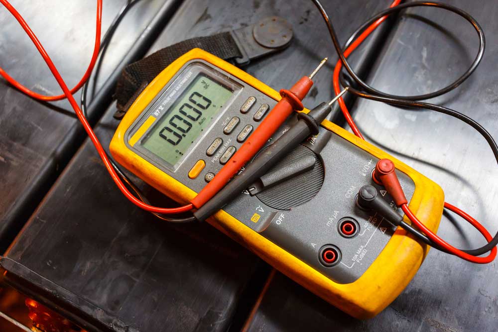
A digital multimeter
So the viable testing methods for modern-day, high-volume production include the following.
Flying probe test
Pinned fixture test
Burn-in test
Automated optical inspection
X-ray inspection
Automated optical inspection of a PCB by a factory worker
Wrap Up
In conclusion, bare printed circuit boards are more viable for the mass production of electronics than unique PCBs because they have the versatility and flexibility advantage. And we have the experts to help you actualize your board from the design files. Contact us for more details if you want a high-quality PCB or PCBA for your project.
Comment on this article here
-
No comment

Ripple
Hi everyone, I'm Ripple, Sales Director of KFPCBA Tech Ltd. If you are looking for a one-stop PCB and PCB assembly manufacturer in China, KFPCBA is your best choice! Please feel free to contact our team! Thanks!
Contact me now
Relevant content you may be interested in
Related articles


