


 tel:+86-18825224069
 email:
 address:201, Factory 6, Longhui Industrial Park, Fuqiao 3rd District, Xinhe Community, Fuhai Street, Baoan District, Shenzhen china
What information do I need to provide for SMT patch proofing?
Release date:2021-12-08 17:04:02 Number of views:0
As a professional PCBA proofing platform, we often encounter incomplete information provided by many customers, leading to delays in delivery. In order to save time and improve production efficiency, the editor will share today: The information that needs to be provided in SMT patch proofing is: Which ones?
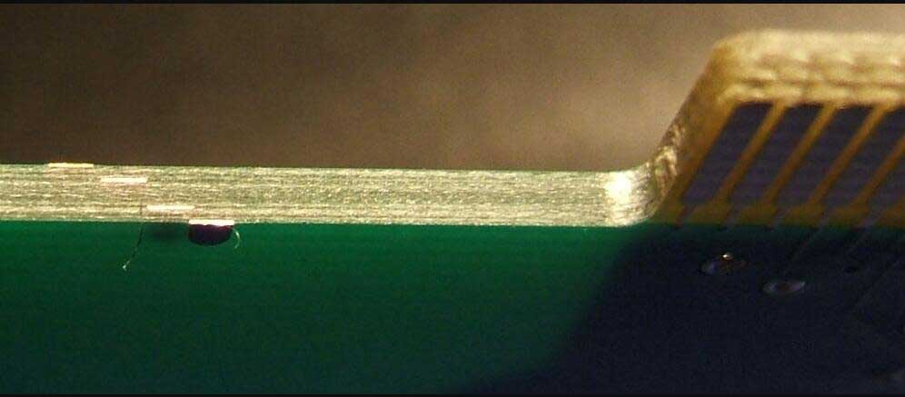
Gerber data file: If you choose an SMT patch processing plant for placement, you need the Pad layer, solder mask layer, silk screen layer, and stencil layer in the Gerber data when opening the stencil and making the patch process; if only SMT is required When the assembler is engaged in the OEM business, it only needs to provide the documents required by the processing factory of the SMT OEM; if your board is a jigsaw, you need to provide the jigsaw file.

BOM: It is the bill of materials, which contains the actual required bill of materials when performing SMT patch proofing. The information must be detailed and accurate. If there is any change, it should be noted on the BOM.
Coordinate file: Need to provide the origin of the PCB board for SMT patch processing, which is generally placed in the lower left corner of the design. It also needs to describe the position information of the components. The extension is .txt or Excel format; the unit is metric, and the default is mm (millimeter) .
Location map file: The pad and silk screen layer of the PCB file exported from the R&D software, SMT placement is used to check whether the placement of the SMT material is correct.
Test guidance documents: guidance and technical requirements for professional parameters in testing.
The above is the introduction to the information required for SMT patch proofing. As a professional PCBA smart manufacturing service platform, Kuaifa Zhizhi provides online quotation, order placement, payment, order inquiry and other services, focusing on SMT patch proofing, PCB proofing, and yuan One-stop service such as device purchasing.
Comment on this article here
-
No comment

Ripple
Hi everyone, I'm Ripple, Sales Director of KFPCBA Tech Ltd. If you are looking for a one-stop PCB and PCB assembly manufacturer in China, KFPCBA is your best choice! Please feel free to contact our team! Thanks!
Contact me now


