


 tel:+86-18825224069
 email:
 address:201, Factory 6, Longhui Industrial Park, Fuqiao 3rd District, Xinhe Community, Fuhai Street, Baoan District, Shenzhen china
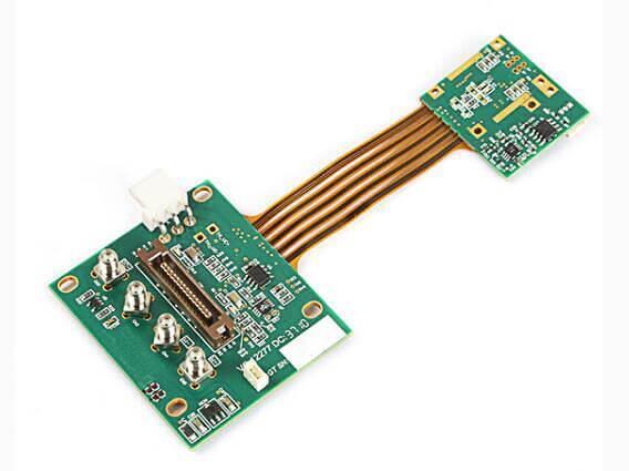
Classification And Production Methods Of Printed Circuit Boards
Release date:2023-02-16 15:50:36 Number of views:91
Classification and production methods of printed circuit boards -KFPCBA

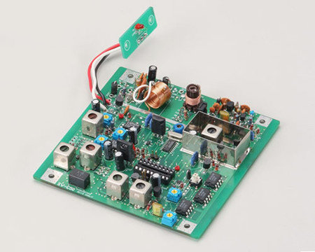
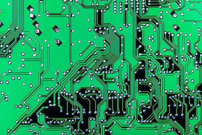
Classification of color printed circuit boards? Color printed circuit boards. Color printed circuit board is a big part of electronic production, and it is also the technology that can best demonstrate the production level of electronic enthusiasts. Color printed circuit board is referred to as printed board. There is a big difference between shoe factory production and amateur production. Shoe factories usually follow the The circuit schematic diagram provided by the customer is used to design a color-printed board diagram with a computer, and then the printed board is made through photographic plate-making and other technologies, and then solder masking, printing, etc. are applied to produce finished products, which require a series of equipment. In the traditional amateur production, only copper-clad boards and corrosive liquids can be used to make printed boards. In recent years, new technologies such as universal test boards and photosensitive circuit boards have been introduced, which have liberated the vast number of electronic enthusiasts and electronic product development. Coupled with the popularity of PCs, it is not difficult to design circuits with CAD software and automatically generate PCBs (color printed circuit boards). I used ORCAD software in the course school of middle school, and used it to design a typical application circuit of 8031 single-chip microcomputer. I think it is really good. The teacher is not allowed to use the manual wiring function of ORCAD. The manual wiring of that picture is beautiful. The corner of the wiring They are all smooth transitions, fully considering that this design makes the printed board more reliable, so that the teacher thought it was manual wiring (not boasting:-) Unfortunately, there was no copier to copy the PCB at that time. It is well known to the majority of electronic enthusiasts, but it is a pity that there is no deep research on it. The usual electronic manufacturing circuits are not complicated. Let's talk about the traditional way of making printed boards.
First of all, design a color printed circuit board diagram on paper according to the circuit schematic diagram. The correct connection between components is important, and attention should also be paid to the size, arrangement, interference, etc. of components (a special article will be written later) Describe how to design a printed board) After the design is completed, it is necessary to repeatedly check the schematic diagram, find out the actual components and place them in their respective positions, pay attention to the front and back when adjusting the hole spacing, routing, etc. Put the picture on the carbon paper and trace it once, so that you have what you need on the reverse side of the paper. The way to make a printed board is to cut out the designed 1:1 drawing, paste it on the copper surface of the single-sided copper-clad board with transparent glue, and then use a punch to knock on the place where the hole needs to be drilled. , to produce a small pit, so that it will not be locked when drilling with a small electric hammer, and then use a homemade small electric hammer (installed with a tape recorder motor) to make holes, tear off the drawing after all punching, and dip it directly with a pen Paint trace lines. Because the positioning of the holes already exists, it is not difficult to draw, just remember that the holes are connected together ), if it is a complex circuit, you can sandwich a piece of carbon paper between the drawing and the copper-clad board, and then trace the color-printed board diagram, draw the hole deeper, and then use a pen dipped in paint to trace the circuit. If there is no paint, you can use a better quality marker pen to trace the line, or use a correction fluid to trace the circuit board, but the circuit board traced by the correction fluid is not very beautiful, and it needs to be dried to correct the same length. Toenail polish can also be used. It is better to use some correction fluid when drawing, pay attention to keep the distance between the waistlines, and surround the holes to facilitate welding.
It takes a long time for the paint to dry. After the paint is dry, it can be put into the corrosive solution. The corrosive solution is usually made of ferric chloride and salt. Acetonitrile is an earthy red solid, which is also easy to absorb moisture in the air. , so it should be sealed and stored. When configuring phenol lye, usually 40% phenol and 60% water are used. In fact, there is less ferric chloride, or cold water (not cold water, to prevent the paint from cracking) can make the reaction rate faster. Note that phenol is corrosive to a certain extent, it is best not to get it on the skin and clothes (it is difficult to wash:-(use a cheap plastic basin for the reaction container, and it is good to put the circuit board. The corrosion starts from the edge, when After the unpainted copper strip is corroded, the circuit board should be taken out in time to prevent the useful lines from being corroded after the coating cracks. At this time, rinse with clean water, and scrape off the coating with bamboo chips by the way (at this time, the coating comes down from the liquid , easier to remove) If it is not easy to scratch, just rinse it with cold water and then wipe it off, polish it with sandpaper, and the shiny copper strip will be exposed. A color printed circuit board is ready. In order to preserve the results, rosin is generally used Apply lye to the polished circuit board once, which can not only help soldering, but also avoid oxidation. Tomorrow, the editor will talk about the classification of color printed circuit boards? Let’s study it together!
Classification of color printed circuit boards
Color printed circuit board.
Color printed circuit board is a big part of electronic production, and it is also the technology that can best demonstrate the production level of electronic enthusiasts. Color printed circuit boards are referred to as printed boards for short, and shoe factory production is very different from amateur production. Shoe factories usually use computers to design color-printed boards according to the circuit schematic diagrams provided by customers, and then make printed boards through photographic plate-making and other technologies, and then apply solder mask and printing to produce finished products, which require a series of equipment. .In the traditional amateur production, only copper-clad boards and corrosive liquids can be used to make printed boards. In recent years, new technologies such as universal test board and photosensitive circuit board have been introduced, which have liberated a large number of electronic enthusiasts and electronic product developers. Coupled with the popularity of PCs, it is not difficult to design circuits with CAD software and automatically generate PCBs (color printed circuit boards). It is even more convenient to directly copy on the film and cooperate with the photosensitive circuit board to make a color printing plate. . I used ORCAD software in the course school of middle school, and used it to design a typical application circuit of 8031 single-chip microcomputer. I think it is really good. The teacher is not allowed to use ORCAD's manual wiring function. The manual wiring in that picture is beautiful, and the corners of the wiring are smooth transitions. Fully considering this design makes the printing board more reliable, so that the teacher thought it was manual wiring. (Not bragging :-). It's a pity that there was no copier to copy the PCB at that time. . It is well known by the majority of electronic enthusiasts, but it is a pity that there is no deep research on it.
The usual electronic manufacturing circuits are not complicated. For veterans, they only need to use their heads to design color printed circuit board diagrams, so let's talk about the traditional way of making printed boards. .First of all, it is necessary to design a color-printed circuit board diagram on paper according to the circuit schematic diagram. The correct connection between components is important, and attention should also be paid to the size, arrangement, and interference of components. (I will write a special article about how to design printed boards later.) After the design is completed, it is necessary to repeatedly check the schematic diagram, find out the physical components and place them in their respective positions, and adjust the hole spacing, wiring, etc. Pay attention to the front and back. Sometimes you accidentally design the back. You can put the original picture on the carbon paper and trace it once, so that you will have what you need on the back of the paper. .The way to make printed boards is to cut out the designed 1:1 drawings, paste them on the copper surface of the single-sided copper-clad board with transparent glue, and then use a punch to knock on the place where holes need to be drilled to produce concave holes. The small hole that goes in, so that it will not be locked when drilling with a small electric hammer. After that, I used a self-made small electric hammer (additional to the motor of the tape recorder) to punch holes. After all the holes were punched, the drawings were torn off, and the lines were directly drawn with a pen dipped in paint. .Because the positioning of the holes already exists, it is not difficult to draw, just remember that the holes are connected together. Usually uncomplicated circuits can be made in this way very quickly (even carbon paper is saved:-), if it is a complex circuit, a piece of carbon paper can be sandwiched between the drawing and the copper clad board, and then the color printed board is traced again. The place where the hole is punched is drawn darker, and then the line is drawn with a pen dipped in paint.
.If there is no paint, you can use a better quality marker pen to trace the circuit, or use a correction fluid to trace the circuit board, but the circuit board traced by the correction fluid is not very beautiful, and the length needs to be corrected after drying. Toenail polish can also be used, it dries faster and is better than correction fluid. When drawing, pay attention to keep the distance between the waistlines, and surround the holes to facilitate welding. .It takes a long time for the paint to dry. After the paint is dry, it can be put into the corrosive solution. The corrosive solution is usually made of ferric chloride and salt. Acetonitrile is an earthy red solid, which is also easy to absorb moisture in the air, so it should be Keep airtight. When preparing phenol lye, 40% phenol and 60% water are usually used. In fact, less ferric chloride, or cold water (not cold water, to prevent the paint from cracking) can make the reaction faster. Note that phenol is corrosive to a certain extent, it is best not to get it on the skin and clothes (it is difficult to wash:-(use a cheap plastic basin for the reaction container, just put the circuit board in it. Corrosion starts from the edge, When the unpainted copper strip is corroded, the circuit board should be taken out in time to prevent the useful circuit from being corroded after the coating cracks. At this time, rinse with clean water, and scrape off the coating with bamboo chips by the way (at this time, the coating is removed from the liquid If it is not easy to scratch, just rinse it with cold water. Then wipe it off and polish it with sandpaper to reveal the bright copper strip. A color printed circuit board is ready. In order to preserve the results , Generally, the polished circuit board will be coated with rosin lye, which can not only help soldering, but also avoid oxidation.
,
Comment on this article here
-
No comment

Ripple
Hi everyone, I'm Ripple, Sales Director of KFPCBA Tech Ltd. If you are looking for a one-stop PCB and PCB assembly manufacturer in China, KFPCBA is your best choice! Please feel free to contact our team! Thanks!
Contact me now
Relevant content you may be interested in
Related articles


