


 tel:+86-18825224069
 email:
 address:201, Factory 6, Longhui Industrial Park, Fuqiao 3rd District, Xinhe Community, Fuhai Street, Baoan District, Shenzhen china
Circuit design The Simulation Experiment Verifies The Half-bridge LLC Converter And Its Feasibility
Release date:2022-11-18 14:04:38 Number of views:61
The simulation experiment verifies the half-bridge LLC converter and its feasibility
Abstract: LLC converter is a very promising topological circuit. However, its working process is relatively complicated, and it is difficult to establish an accurate small-signal model, so it is difficult to design a closed-loop control circuit. At the same time, with the widespread use of LLC converters, its over-current protection issues are increasingly concerned. Aiming at an improved half-bridge LLC converter with overcurrent protection function, a compensation circuit design method based on Saber software time domain simulation is proposed, and a 1 200 W half-bridge LLC converter is designed. Simulation experiments have verified the correctness and feasibility of the method, which has certain guiding significance for practical engineering applications.
Keywords: LLC converter; compensation circuit; closed-loop control; time domain simulation
0 Preface
The LLC resonant DC converter has the advantages of high efficiency, high power density, and low EMI noise because it can realize the ZVS (Zero) of the primary switching tube and the ZCS (Zero) of the secondary rectifier diode, and has received extensive attention in recent years. [1-2]. Scholars at home and abroad have conducted in-depth research on its topology [3], resonant network parameter optimization design [4-5], control strategy [6-7], and magnetic integration [8]. In order to obtain a good steady-state index and dynamic index, it is usually necessary to introduce a feedback control link when designing a switching converter. However, since the LLC converter is a strongly nonlinear system, its working process is very complicated, and it is difficult to establish an accurate small-signal model [9-10]. At the same time, with the widespread use of LLC converters, its over-current protection issues are increasingly concerned [11-12]. Based on this, for an improved half-bridge LLC converter with self-limiting function [12], this paper proposes a method of using Saber simulation to assist in the design of a closed-loop feedback control circuit, and designs a 400 V input, 48 V output The half-bridge LLC converter is verified.
1 Principle of the improved half-bridge LLC converter
There are some problems in the practical application of LLC converters, one of the main problems is how to effectively suppress the overshoot of the primary side resonant current when the circuit starts up, the load is overloaded or short-circuited. Figure 1 is a topological structure diagram of an improved half-bridge LLC converter with active current limiting function. The two main switches Q1 and Q2 together form a half-bridge structure, which is complementary to conduct with a 50% duty cycle (including dead time). Compared with the traditional half-bridge LLC converter, the improved type still consists of resonant inductor Lr, resonant capacitor Cr, and excitation inductor Lm to form a resonant network, but the resonant capacitor Cr is divided into two parts, Cr1 and Cr2, and connected with clamping diodes. This design will bring two benefits: (1) The split resonant capacitor will reduce the input current ripple, make the resonant current waveform close to sinusoidal, and reduce EMI noise; (2) The parallel diode will actively clamp when overloaded bit, which limits the voltage across the resonant capacitor, so that the resonant current is also clamped to prevent circuit damage.
The steady-state analysis of the half-bridge LLC converter is carried out using the fundamental wave analysis method (FHA), and its DC voltage gain characteristic curve (as shown in Figure 2) is obtained. The circuit design and development can be divided into three areas: The LLC circuit in area Ⅰ works in an inductive state, and the primary side switch tube can realize ZVS, while the current of the rectifier diode on the secondary side is continuous, cannot cross zero naturally, and is hard turned off; the LLC circuit in area Ⅱ works in an inductive state, and the primary side switch tube can realize ZVS , and the current of the rectifier diode on the secondary side is discontinuous, can cross zero naturally, and can realize ZCS, which is the ideal working area of LLC circuit; the resonant circuit in zone III works in a capacitive state, and the current leads the change of voltage, which can realize ZCS, which is LLC Areas where circuits are not suitable for operation. It can be seen from Fig. 2 that in regions I and II, the DC voltage gain of the converter is a monotonically decreasing function, as long as the switching frequency of the LLC converter is adjusted, the magnitude of the DC output voltage can be changed, so by introducing feedback and controlling the switching frequency, it can be To achieve the purpose of stable output.
2 Small signal model analysis based on Saber time domain simulation
From the above analysis, it can be seen that the LLC converter is a variable frequency modulation converter. In order to design a closed-loop compensation circuit for the LLC converter, it is necessary to obtain the small signal transfer function from the switching frequency fs of the primary side to the output voltage Vo, namely
. However, so far, the existing literature has not given an accurate model of the transfer function, which directly leads to the difficulty in the design of the LLC feedback control loop.
In view of this, the TDSA module (frequency response analyzer) in the Saber software is used to conduct small-signal time-domain simulation analysis of the improved LLC converter open-loop circuit, and the Bode plot of the transfer function P(s) can be obtained directly. The terminal of the TDSA module (the instrument in the lower right corner of Figure 3) injects a frequency-adjustable sinusoidal signal into the circuit to be tested, and the input terminal is connected to the output of the circuit to be tested as a feedback signal. By comparing the signals of the two terminals, the two can be obtained. The gain and phase relationship of , that is, the Bode plot. At the same time, the VCO module (voltage-controlled oscillator) in Saber is used to realize the frequency conversion control of the circuit.
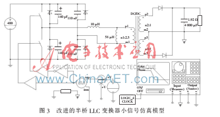
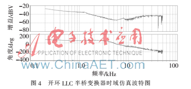
Figure 4 shows the Bode diagram of the control switching frequency to the output voltage of the improved LLC converter at 400 V input, 48 V output, switching frequency 100 kHz, and working in Zone II. It can be seen from the Bode diagram that since the switching frequency fs of the primary side is opposite to the change direction of the output voltage Vo, the starting point of the phase-frequency curve is near 100°. When the switching frequency of the LLC converter increases, the output voltage of the converter decreases accordingly. The analysis shows that the open-loop circuit of the LLC converter is a high-order system, and its open-loop transfer function has multiple poles and zeros. One of the zeros is formed by the ESR of the capacitor. Usually when designing a closed-loop compensation circuit, in order to have better steady-state error and dynamic characteristics, it is hoped that the corrected system will have larger amplitude-frequency characteristics at low frequencies and a certain phase margin (45°~75°). Since the starting point of the phase-frequency curve is located near 100°, the open-loop system has a large phase lead characteristic in a wide frequency range, resulting in an excessively large phase margin of the original system. The slope of the amplitude-frequency characteristics in the low-frequency band of the original system is -10 dB/dec, so a larger gain is expected to obtain better dynamic characteristics. The amplitude-frequency characteristic slope of the mid-frequency band in the original system is -40 dB/dec, which meets the requirements without compensation. In the high-frequency band, the phase-frequency characteristics of the original system have large oscillations, which brings unstable factors to the system. Therefore, it is hoped that the corrected system can drop as fast as possible in the high-frequency link, and at the same time it is beneficial to suppress high-frequency switching. noise.
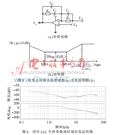
Reference [9] pointed out that the small-signal modeling of the LLC converter can be carried out by the extended description function method, and the zero-pole distribution of the open-loop transfer function of the system can be obtained, and it is pointed out that in area I there is a parameter related low frequency pole, a double pole and a zero related to the ESR of the capacitor. When the switching frequency is close to the resonant frequency, one moves to the high frequency and one moves to the low frequency pole. When the load changes, the closed-loop controlled LLC converter will adjust the voltage gain to change the output by changing the frequency, so in fact, the LLC converter may also work in zone I as the load changes at this time. Considering comprehensively, a double-zero double-pole compensator is selected here (the compensation circuit and Bode diagram are shown in Figure 5), which combines the characteristics of lead compensation and lag compensation, and uses the characteristics of lag compensation to improve static performance. Using the characteristics of lead compensation to improve relative stability and dynamic performance. The transfer function corresponding to the double-zero and double-pole compensation circuit is shown in formula (1), through the turning point
The frequency setting can realize the compensation of each frequency segment conveniently and flexibly. By changing
The value of , can move the Bode plot of the system transfer function up and down, thus changing the gain and phase margins. In this way, the design of the system closed-loop compensation circuit can be realized conveniently. The Bode plot of the closed-loop system after compensation is shown in Figure 6.
At the same time, there is another advantage of choosing a double-zero-point double-pole compensation circuit, that is, it is easy to obtain its Z-domain transformation equation (as shown in formula (1)), and it can be easily differentiated, easy to be implemented in DSP system programming, and the corresponding differential The equation is shown in formula (3).
u(k)=b0e(k)+b1e(k-1)+b2e(k-2)-a1u(k-1)-a2u(k-2) (3)
3 Simulation experiment verification
Based on the time-domain simulation of Saber software, a closed-loop half-bridge LLC converter with a rated operating frequency of 100 kHz, a rated input of 400 V, and a rated output of 1200 kW (48 V/25 A) is designed for experimental verification. Circuit parameters: Lr=10 μH, Lm=58 μH, Cr1=110 nF, Cr2=110 nF, filter capacitor Co=4 000 μF, transformer turns ratio 2.5:1. Figure 7 shows the output voltage waveform when the open-loop circuit is fully loaded, and it can be seen that its overshoot is nearly 20%. Figure 8 is the waveform of the output voltage when the closed-loop circuit is fully loaded and switched to half load in 0.025 s, and Figure 9 is the corresponding resonance current waveform in this case. The simulation results show that the designed circuit can achieve good steady-state and dynamic indicators at full load and half-load, and there is no current overshoot peak in the resonant current waveform, indicating that the improved LLC topology circuit has reached the peak value when the circuit starts. Active current limiting protects circuit components.
4 Conclusion
The working process of LLC resonant converter is complex, and small signal modeling is difficult. In this paper, Saber is used to simulate a half-bridge LLC converter with self-limiting function in time domain, and a simplified small signal model is obtained to realize the closed-loop feedback compensation circuit. The design of the simulation experiment verifies the correctness and feasibility of the method.
references
[1] YANG B, LEE FC, ZHANG AJ, et al. LLC for front end DC/DC [C]. IEEE, Power and , APEC 2002, 2002, 2: 1108-1112.
[2] Fu , LEE FC, Liu Ya, et al. Novel multi- for front-end DC/DC [C]. of IEEE Power , PESC 2008, 2008: 250-256.
[3] Yang Bo. for front end DC/DC power for power [D]. and State , USA, 2003.
[4]. LLC half- [S]. 2009.
[5] Lu Bing, Liu , Liang Yan, et al. for LLC [C]. -First IEEE Power and , 2006, APEC′06, 2006: 533-538.
[6] JU W C. LLC DC/DC with PLL [D]. Cheng Kung, 2006.
[7] Hang Lijun, Lu, Qian. of for multi-LLC [C]. IEEE on, 2007: 479-484.
[8] Yang Bo, Chen, LEE F C. for LLC [C]. IEEE Power and , APEC 2002, 2002, 2: 346-351.
[9] YANG E X. for small-of and multi- [J]. , Tech, Blacksburg, VA, 1994.
[10] LAZAR, R. Stedy-state of the LLC [C]. IEEE Power and , APEC 2001, 2001, 2: 728-735.
[11] Xie, Zhang Circuit Design and Development , Zhao Chen, et al. and of LLC with a novel over [J]. IEEE on Power, 2007, 22: 435-443.
[12] YANG B, LEE FC, M. Over for LLC [C]. of 18th IEEE Power and , 2003: 605-609.
Comment on this article here
-
No comment

Ripple
Hi everyone, I'm Ripple, Sales Director of KFPCBA Tech Ltd. If you are looking for a one-stop PCB and PCB assembly manufacturer in China, KFPCBA is your best choice! Please feel free to contact our team! Thanks!
Contact me now


