


 tel:+86-18825224069
 email:
 address:201, Factory 6, Longhui Industrial Park, Fuqiao 3rd District, Xinhe Community, Fuhai Street, Baoan District, Shenzhen china
PCB And Circuit Design, Sharing Expert Solutions
Release date:2023-02-27 11:42:26 Number of views:137
Some key points of PCB and circuit design , sharing expert solutions
PCB design is intricate, and various unexpected causes will also affect the achievement of the overall plan. In order to produce high-quality PCB boards in volume without reducing design time and causing costly rework, design and circuit integrity issues must be detected as soon as possible in the design process.
However, there are a lot of small details in the PCB design process. If some small details are not paid attention to, it may greatly affect the performance of the entire PCB, and even determine the success or failure of the entire product. What other details should we focus on in order to maximize design efficiency and product quality?
In the previous article, we have already counted some key points of hole slot and circuit design for you through actual cases.
In the process of actually connecting with customers, we also summed up some points for attention in character, shape, and jigsaw design. As a high-reliability multi-layer board manufacturer, KFPCBA focuses on PCB development and manufacturing, providing customers with high-reliability and short-term delivery board experience.
"Cost reduction and efficiency increase for the electronics industry" is our mission. We know that in the main production chain, the cost of product design, development and design engineering does not account for a high proportion, but it will have a great impact on the total cost. In view of the important role of the product design stage in the quality and cost of the final product, the following will combine actual cases of character, shape, and panel design to share expert solutions to some problems in the design, so as to promote the cost reduction and efficiency increase of the whole process.
01
Character Design Case 1: Standardization of Character Design
question:
The general industry is the design and production of machine-mounted PCBs . The requirements for labeling PCB design and production are not high, but from an engineering point of view, for characters with upper window vias, it will be judged as abnormal design, and it will take time to communicate back and forth with EQ.
Expert advice:
For the convenience of repairing and spot welding, the tag numbers are placed outside the component frame, and the tag numbers are placed or not placed in order in dense areas.
02
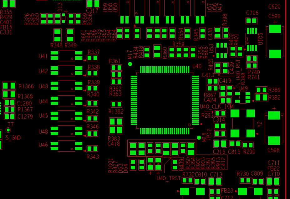
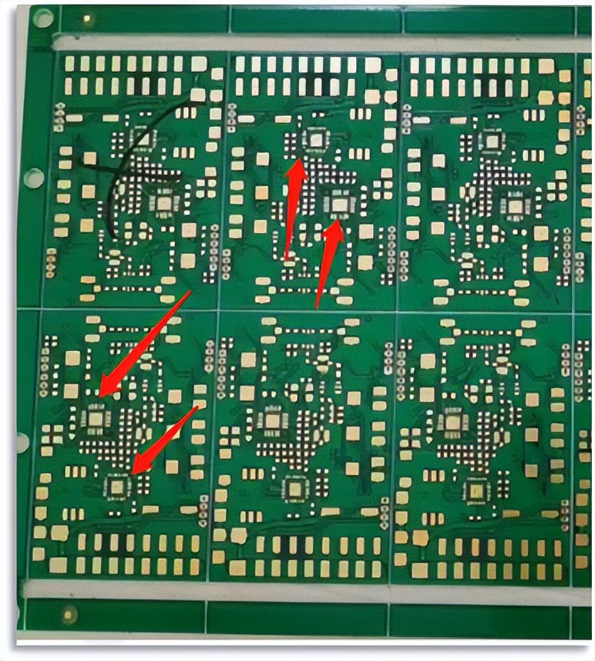
Appearance Design Case 1: Considerations when designing internal milling slots
The problem of whether the actual milling cutter can enter & production efficiency
Problem: In the design document provided by the customer, the inner groove needs to be hollowed out, but the width of the arch is higher than 0.8mm, and the conventional milling cutter cannot enter it.
Expert advice: without affecting the function of this board, customers can be advised to strengthen the distance at the arc; place a "cleaning corner hole" at the concave corner (see the red arrow in the picture)
03
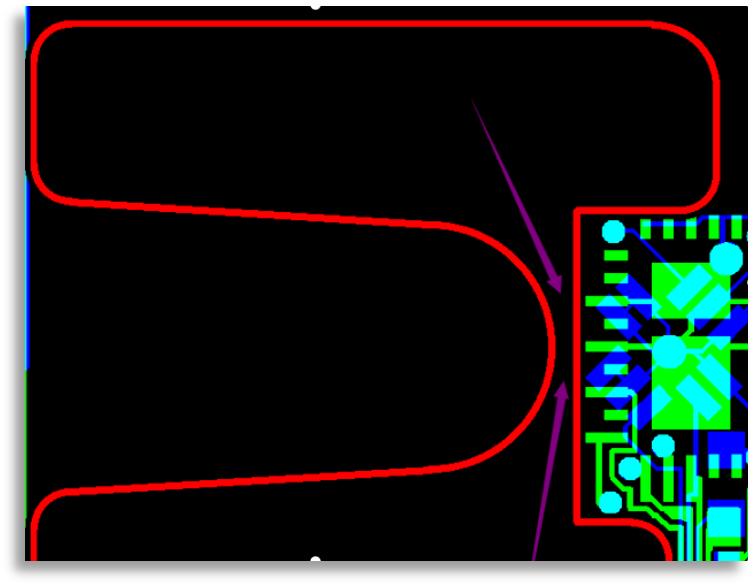
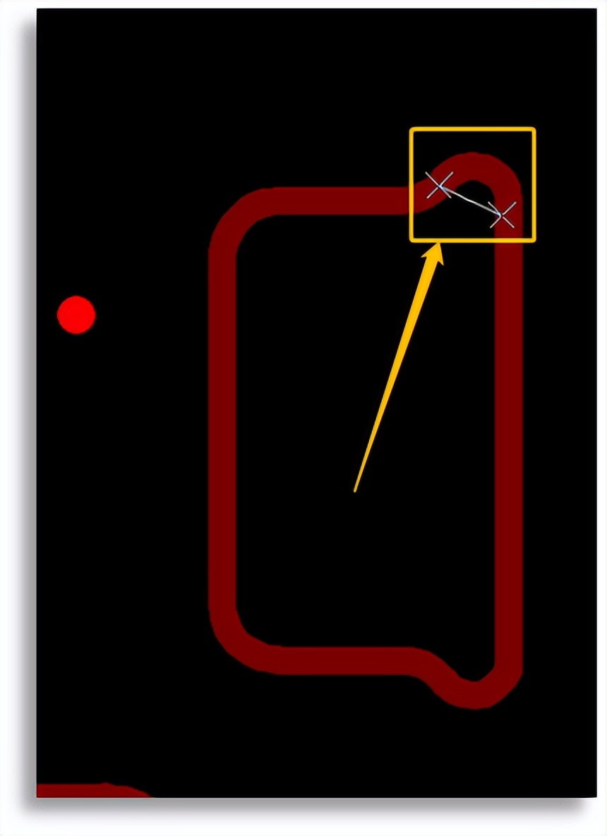
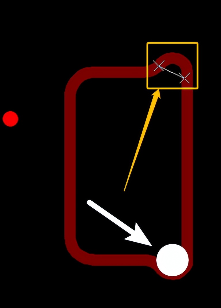
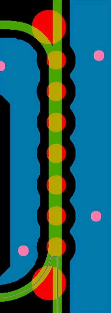
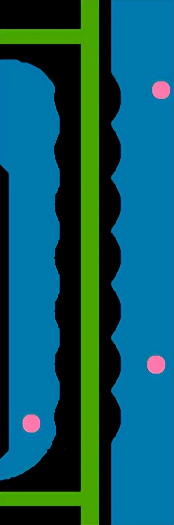
Appearance design case 2: Detailed design of board edge joints
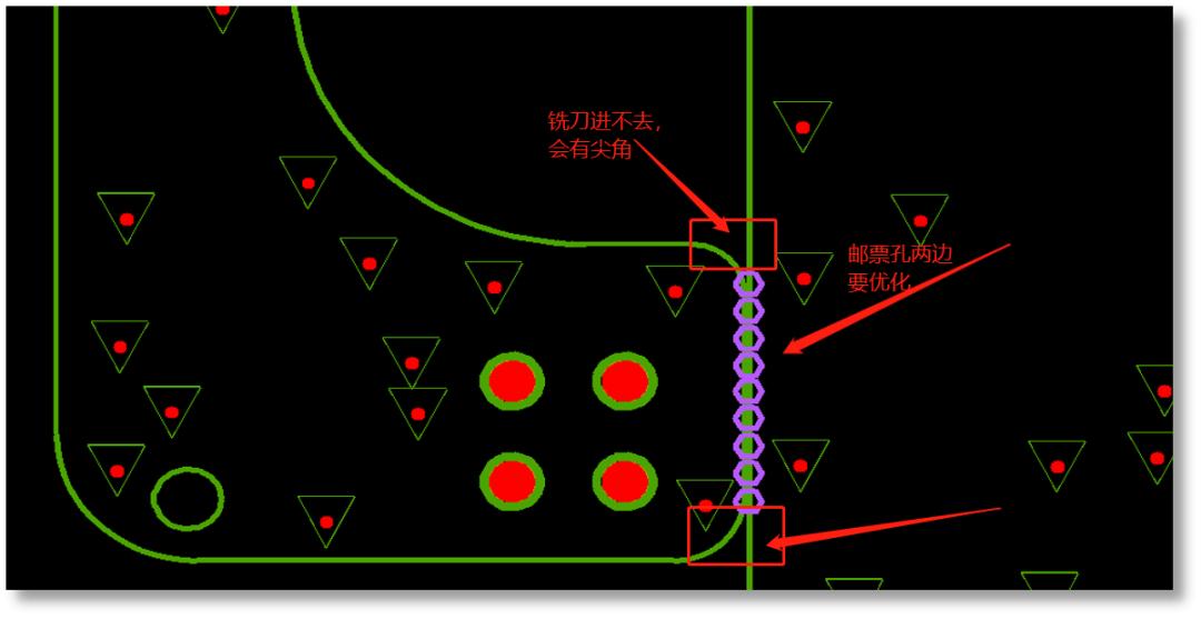
Problem: When designing the board edge connection, two adjacent boards have rounded corners on one side, straight sides on the other, and postage holes in the middle. When the milling cutter cuts, it will cause sharp corners on the back of the boards, which need to be brazed Afterwards, it is ground into rounded corners; from the front end, it is usually to drill holes at both ends of the stamp hole. The drilling will cause slight damage to the board and usually affect the product, and in terms of PCB standards, it may be form a dispute
Expert advice: Without affecting the structure, it is recommended to change the rounded corners to right angles or add "corner clearing holes" to reduce production efficiency and make the finished board more beautiful.
04
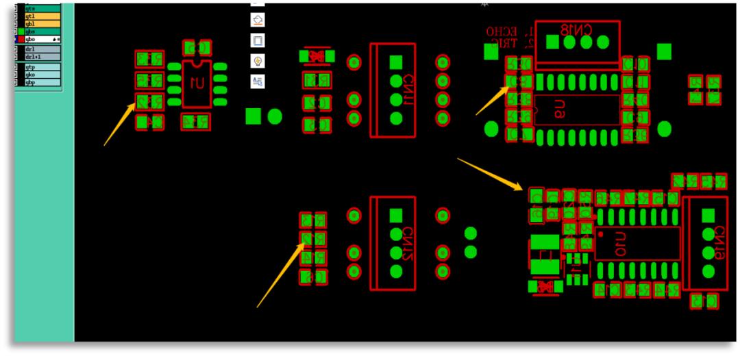
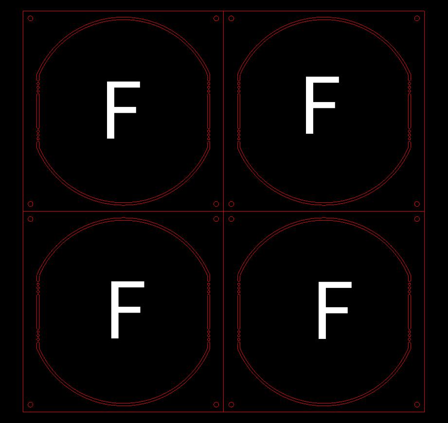
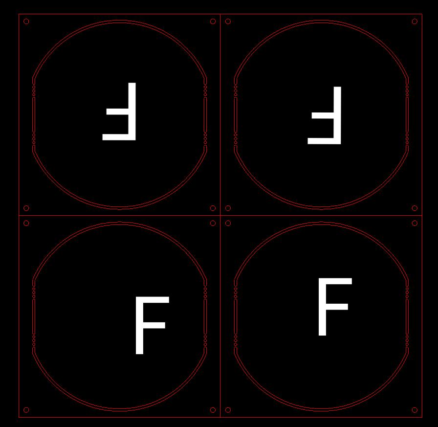
SET jigsaw puzzle design case 1: expression of jigsaw puzzle direction
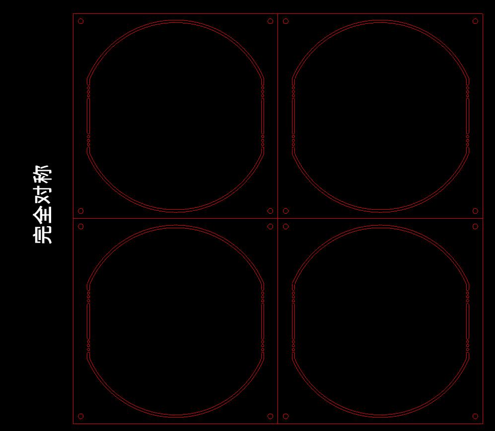
Question: To express the direction of the panel, the customer provides a schematic diagram of the imposition that is similar to the complete symmetry of the left picture above, or provides a reference to the physical picture similar to the picture above and below, which does not clearly indicate the direction of the panel. If you do not look carefully at the small component symbols in the middle, It is difficult for the front-end personnel to know that it is a double fight, and it is easy to mistake it for a straight fight, resulting in component interference and failure to braze during brazing.
Expert advice: From a standard point of view, clear direction marking is required on design documents (except for asymmetrical documents)
The above are several PCB design details optimization cases. As an industrial digital service platform aimed at improving the service model of the traditional electronics industry chain with information technology, KFPCBA optimized the above four actual cases in the process of receiving orders. High-reliability products + visual delivery experience + reliable service are our commitments to global customers. Really carry forward the original intention and mission of "reducing costs and increasing efficiency for the electronics industry" with actions!
In the future, we will continue to share more knowledge about electronic circuit manufacturing and assembly". If you have any questions, or need support, please contact us, and you are welcome to continue to pay attention to KFPBBA.
Comment on this article here
-
No comment

Ripple
Hi everyone, I'm Ripple, Sales Director of KFPCBA Tech Ltd. If you are looking for a one-stop PCB and PCB assembly manufacturer in China, KFPCBA is your best choice! Please feel free to contact our team! Thanks!
Contact me now
Relevant content you may be interested in
Related articles


