 address:201, Factory 6, Longhui Industrial Park, Fuqiao 3rd District, Xinhe Community, Fuhai Street, Baoan District, Shenzhen china
circuit maker 2022How to update pcb from schematic
At this stage of pcb board design, it is necessary to transfer data from the schematic editor to the board editor, the location of components, taking into account the technical specifications and the formation of the topology of printed conductors. Therefore, issues related to the parallel operation of the circuit - the board will also be considered.

While AltiumDesigner has automatic and semi-automated board placement tools, any experienced designer knows that no software can place components on a board better than a human. Given the low efficiency of automatic placement, the article will consider only manual and semi-automatic placement tools, which include the tools of the Tools > ComponentPlacement group.
Updating PCB from Schematic Altium
A big role here is played by the so-called. "Rooms" - areas of the board, to which certain groups of components are assigned. When transferring information from a schematic to a board, Altium Designer automatically generates rooms on the board, unless this is disabled in the settings.
Rooms are formed according to the sheets of the scheme, and it is most advisable to use rooms in cases where when there are repeating fragments of the circuit since by tracing in one “room” it can be duplicated in the rest. More details about "rooms" and their properties will be discussed in another article.
Logical Blocks in Schematic Altium
A multi-sheet project is formed as a hierarchical structure of logical blocks, where each block can be either a schematic sheet or an HDL file (VHDL or Verilog). At the head of this structure is the single master sheet of the schematic, more commonly referred to as the top sheet of the design.
The sheet structure itself is formed using special symbols called the schematic sheet symbol. Each of the source documents that define the project is represented on the top sheet with a sheet symbol.
The name of each sheet symbol refers to the underlying schematic file (or HDL file) that it represents graphically. On the other hand, a sub-schema may also contain further sheet symbols that refer to lower-level schematic sheets or IIDL files. Thus, it is possible to form a structural hierarchy of source documents, which can be simple or complex, depending on the need for the task.
When compiling a multi-sheet project, the logical relationships between the modular blocks of the project are implemented and a structural framework is created. This is a tree structure. starting with a top-level schema sheet and branches to reflect all other subordinate schemas.
As an electronic device, within the framework of this article, the design of the remote control (RC) for a digital camera is used. The circuit is located on one sheet and therefore when transferring data from the schematic editor to the PCB editor, one “room” will be formed.
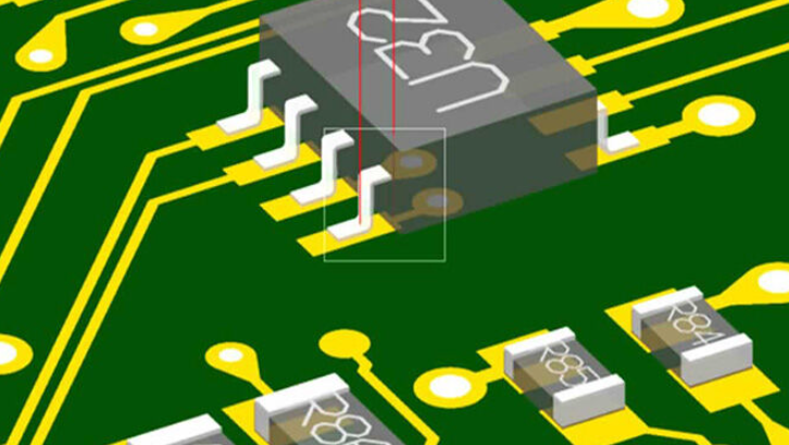
Why it is important to create pcb blanks in schematic design?
Before you can transfer information from the schematic editor to the PCB editor, you must create a PCB blank. To solve this problem, use the File>New>PCB command
And before you continue to work, you must immediately save the project, for which you need to right-click on it and select Save As from the context menu ... We save it in the same folder where the project is called "PCB_ProjectTEST"
It is worth noting that if the board is created using the PCB Board Wizard, then it must be connected to the project. To do this, while in the Projects panel, simply drag the PCB document to the project by holding it with the left mouse button.
Transfer pcb schematic design
When transferring schematic information to a new board layout, ensure that all schematic and board-related libraries are connected and accessible. Once the integrated libraries are installed, the footprints used in this tutorial will be enabled by default.
To transfer the schematic information of the design to the board, you must perform the following steps:
Switch to the schematic editor by selecting the open schematic tab at the top or by double-clicking on the schematic name PCB_ProjectTEST.SchDoc in the Projects panel.
Right-click on any component on the schematic sheet: In the context menu, execute the command Find Similar Objects.
In the window that appears, make sure that the Same operator is set in the Object Kind field, and all options are enabled at the bottom of the window, except for Create Expression.
In the list of properties of the selected components, in the Object Specific section, set the True operator opposite the Use Library Name line.
Confirm the changes by pressing the ENTER key and closing the window.
Setting the Use Library Name line to True
Now we can transfer the schematic to the PCB editor:
1. Open the PCB_ProjectTEST.SchDoc schema.
2. Execute Design>Update PCB Document (PCB_ProjectTEST.SchDoc.). The project compiles and the Engineering Change Order dialog appears.
3. Click Validate Changes. If all changes are valid, a checkmark appears in the Status>Check column.
If the changes are invalid, close the dialog, check the Message panel and fix any errors.
4. Click Execute Changes to send the changes to the board. Upon completion of this operation, a checkmark appears in the Status column in the Done section.
5. Click Close and the design board will open with components ready for placement.
Board with components
Use the hotkeys V, and D (View Document) if all the components on the diagram are not visible in the current view.
Using the Report Dangles button, you can create an ECO report for printing.
Each enterprise uses its element base of components, which is why standard libraries are not able to fully meet the needs of designers. The problem arises with manufacturing libraries of electronic components intended for a specific production. This article discusses ways to simplify the implementation of this task.
Tip #1
With a schematic file and a PCB file, you can quickly create a library of components that are on the board. A similar situation may arise when importing a project from a third-party CAD system.
Being in the schematic, let's create a library of components used in the project with the Design > Make Schematic Library command
Restoration of the library according to the available data
Save the created library with the File > Save command; It should be noted that all components of the library have a reference to the footprint, but there are no footprints themselves yet. Now, in a similar way, we will create a library of used footprints from the board using the Design > Make PCB Library command.
Restoring the footprint library according to the available data and save it with the File > Save command. It is worth clarifying that when using Altium Designer below version 14, there may be problems with the naming of footprints in these two libraries, in the library, an underscore may be added to the names.
The situation can be corrected by renaming all footprints in the footprint library (.PCBLIB) (the extra character must be removed from the names).
we have a symbol library in which all components have footprints
After creating libraries, the task of making changes to the graphical part of the project may arise. Editing can affect one specific symbol and contain a set of simple procedures, such as changing line thickness or pin numbering. This section will cover issues related to editing multiple components or multiple objects on the same component, i.e. global editing.
When we created the library, we did not yet know what packages our components would have (especially resistors, and capacitors) and connected only the most common packages. It's time to decide on this for the created scheme.
Let's enter the properties of the component. The Footprint selection is made in the Name drop-down menu of the Models window.
Footprint selection
The list contains only those Footprints that we have defined in the library element. If we are not satisfied with it, we can delete it or assign a new one (Edit button). This is quite remarkable since you do not need to bind to models by creating libraries but directly set them in the schema.
If you do not need to edit the Footprint for a large number of circuit elements, it is better to use the Tools / Footprint Manager Command. However, before that, we must install all the Footprint libraries that we will use. To do this, select the components which you want and click the ADD button. Then search for the required Footprint.
Tip #3
After importing from P-CAD, some character lines appear thicker than others and all texts have an anchor point. It is necessary to make all lines of the same thickness and remove the display of the anchor point for all components of the library.
To solve this problem, being in the editing mode of any component of the library, right-click on the designator and call the Find Similar Object command (if the designators are not displayed in the library, you must enable the Always Show Comment/Designator parameter in the Tools > Document Options settings).
Enabling the Always Show Comment/Designator option
In the Find, Similar Object window set the settings following Figure 6, and pay attention to where the objects will be selected. After pressing the OK button, the Inspector panel will start, in which you should also select work with all components.
Before making edits, make sure that the status bar of the Inspector panel shows a total number of tags equal to the number of components in the library. After that, you can put a “daw” in the Auto position field, which hides the anchor point of the text. Similarly, we correct the thickness of the lines for all components of the library.
-
No comment




 tel:+86-18825224069
 email:


