


 tel:+86-18825224069
 email:
 address:201, Factory 6, Longhui Industrial Park, Fuqiao 3rd District, Xinhe Community, Fuhai Street, Baoan District, Shenzhen china
PCB manufacturers share some key points about PCB manufacturing and design
Release date:2022-11-07 16:22:34 Number of views:0
PCB manufacturers share some key points about PCB manufacturing and design
1. Treatment of power supply and ground wire
Even though the wiring in the whole PCB board is well completed, the interference caused by improper consideration of power supply and ground wire will degrade the performance of the product, and sometimes even affect the success rate of the product Therefore, the wiring of electrICal and ground wires should be taken seriously to minimize the noise interference generated by electrical and ground wires to ensure the quality of products.
Every engineer engaged in electronic product design knows the cause of the noise between the ground wire and the power line, and now only describes the reduced noise suppression:
It is well known that a coupling capacitor is added between the power supply and the ground wire.
The width of power supply and ground wire should be widened as much as possible. The ground wire should be wider than the power wire. Their relationship is: ground wire>power wire>signal wire. Generally, the width of signal wire is 0.2~0.3mm, the narrowest width can be 0.05~0.07mm, and the power wire is 1.2~2.5mm.
For PCB of digital circuit, a wide ground wire can be used to form a loop, that is, to form a ground grid for use (the ground of analog circuit cannot be used in this way). A large area of copper layer is used as the ground wire, and the unused places are connected to the ground on the printed board as the ground wire. Or it can be made into a multilayer board, with one layer for power supply and one layer for ground wire.
2. Common Ground Processing of Digital Circuit and Analog Circuit
Nowadays, many PCBs are no longer single functional circuits (digital or analog circuits), but are composed of digital circuits and analog circuits Therefore, when wiring, it is necessary to consider the mutual interference between them, especially the noise interference on the ground wire.
The frequency of digital circuit is high and the sensitivity of analog circuit is strong. For the signal line, the high-frequency signal line is as far away from the sensitive analog circuit device as possible. For the ground wire, the integrated PCB has only one node to the outside world. Therefore, the problem of digital and analog common ground must be handLED inside the PCB. In fact, the digital ground and analog ground inside the board are not connected with each other, Only at the interface between PCB and the outside world (such as plug), there is a short circuit between the digital ground and the analog ground. Please note that there is only one connection point. There is also a non common ground on the PCB, which is determined by the system design.

3. The signal line is laid on the electrical (ground) layer
When wiring multilayer printed circuit boards, there are not many lines left in the signal line layer, so adding more layers will cause waste and increase the workload and cost of production. To solve this contradiction, we can consider wiring on the electrical (ground) layer. First, we should consider using the power layer, and then the stratum. Because it is better to preserve the integrity of the stratum.
4. Treatment of connecting leg in large area conductor
In large-area grounding (electricity), the legs of commonly used components and parts are connected with each other, and the treatment of connecting legs needs to be considered comprehensively. As far as electrical performance is concerned, it is better to fully connect the bonding pad of component legs with the copper surface, but there are some adverse hazards in the welding assembly of components, such as: ① high-power heater is required for welding. ② It is easy to cause false solder joints Therefore, taking into account the electrical performance and process needs, the cruciform bonding pad is made, which is called heat shield, commonly known as thermal bonding pad. In this way, the possibility of false solder joints due to excessive heat dissipation of the cross section during welding can be greatly reduced. The treatment of the electric (ground) leg of the Multilayer board is the same.
5. The role of network system in cabling
In many CAD systems, routing is determined by the network system The grid is too dense, the access is increased, but the step size is too small, and the amount of data in the map field is too large, which will inevitably have higher requirements for the storage space of the equipment. At the same time, the operation speed of computer electronic products will be greatly affected However, some paths are invalid, such as those occupied by the bonding pad of the component leg or by the mounting hole or the fixing hole. Too sparse grid and too few paths have a great impact on the routing rate. Therefore, a reasonably dense grid system is required to support the routing.
The distance between the legs of standard components is 0.1 inch (2.54mm), so the foundation of the grid system is generally 0.1 inch (2.54 mm) or an integral multiple of less than 0.1 inch, such as 0.05 inch, 0.025 inch, 0.02 inch, etc.
6. Design Rule Check (DRC)
After the wiring design is completed, it is necessary to carefully check whether the wiring design conforms to the rules formulated by the designer, and also to confirm whether the rules formulated conform to the requirements of the PCB production process. Generally, the following aspects are checked:
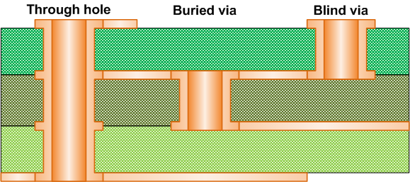
Whether the distance between line and line, line and component pad, line and through-hole, component pad and through-hole, through-hole and through-hole is reasonable and meets Production requirements.
Whether the width of power line and ground wire is appropriate, and whether the power line and ground wire are tightly coupled (low wave impedance)? Is there any place in the PCB where the ground wire can be widened.
Whether the best measures have been taken for the key signal lines, such as the shortest length, adding protective lines, and the input lines and output lines are obviously separated.
Whether the analog circuit and digital circuit have their own independent ground wires.
Whether the graphics (such as icons and labels) added in the PCB will cause signal short circuit.
Modify some undesirable alignments.
Is there a process line on the PCB? Whether the resistance welding meets the requirements of the production process, whether the resistance welding size is appropriate, and whether the character MARK is pressed on the device pad to avoid affecting the electrical installation quality.
Whether the frame edge of the power supply layer in the multilayer board is shrunk, for example, the copper foil of the power supply layer is exposed outside the board, which may cause short circuit The purpose of this document is to describe the process and some precautions of PCB design using PADS PCB design software PowerPCB, and to provide design specifications for designers in a working group, so as to facilitate communication and mutual inspection between designers.
Comment on this article here
-
No comment

Ripple
Hi everyone, I'm Ripple, Sales Director of KFPCBA Tech Ltd. If you are looking for a one-stop PCB and PCB assembly manufacturer in China, KFPCBA is your best choice! Please feel free to contact our team! Thanks!
Contact me now
Relevant content you may be interested in
Related articles


