


 tel:+86-18825224069
 email:
 address:201, Factory 6, Longhui Industrial Park, Fuqiao 3rd District, Xinhe Community, Fuhai Street, Baoan District, Shenzhen china
pcb antenna connector: Wireless Devices for Receiving and Transmitting Signals
Release date:2022-06-01 16:55:08 Number of views:0
Wireless devices are becoming the norm for most applications, so there is a high demand for PCB antennas to enable seamless communication. Think of simple devices like wireless mice to the emerging 5G network and IoT. These require wireless communication, and a PCB antenna will be instrumental in their development. If you are working on a project involving wireless connectivity, here is a close look at PCB antennas, including their types and how to design one. Let's dive in!
Contents [hide]
Types of Antenna
Antenna Parameters
How to Design a PCB Antenna
Types of Antenna Printed Circuit Boards
Summary
Types of Antenna
The following are the three antenna types.
Wire Antennas
A wire antenna is essentially a cable that extends above the PCB in free space. It gives the best range and performance due to its 3D exposure and dimensions.

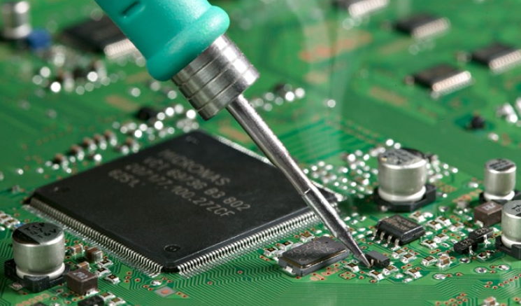
PCBA Wi-Fi Card with Wire Antenna
Source: Wikimedia Commons
PCB Antenna
Also known as a PCB trace antenna, this PCB antenna type is as simple as a trace drawn on the circuit board.
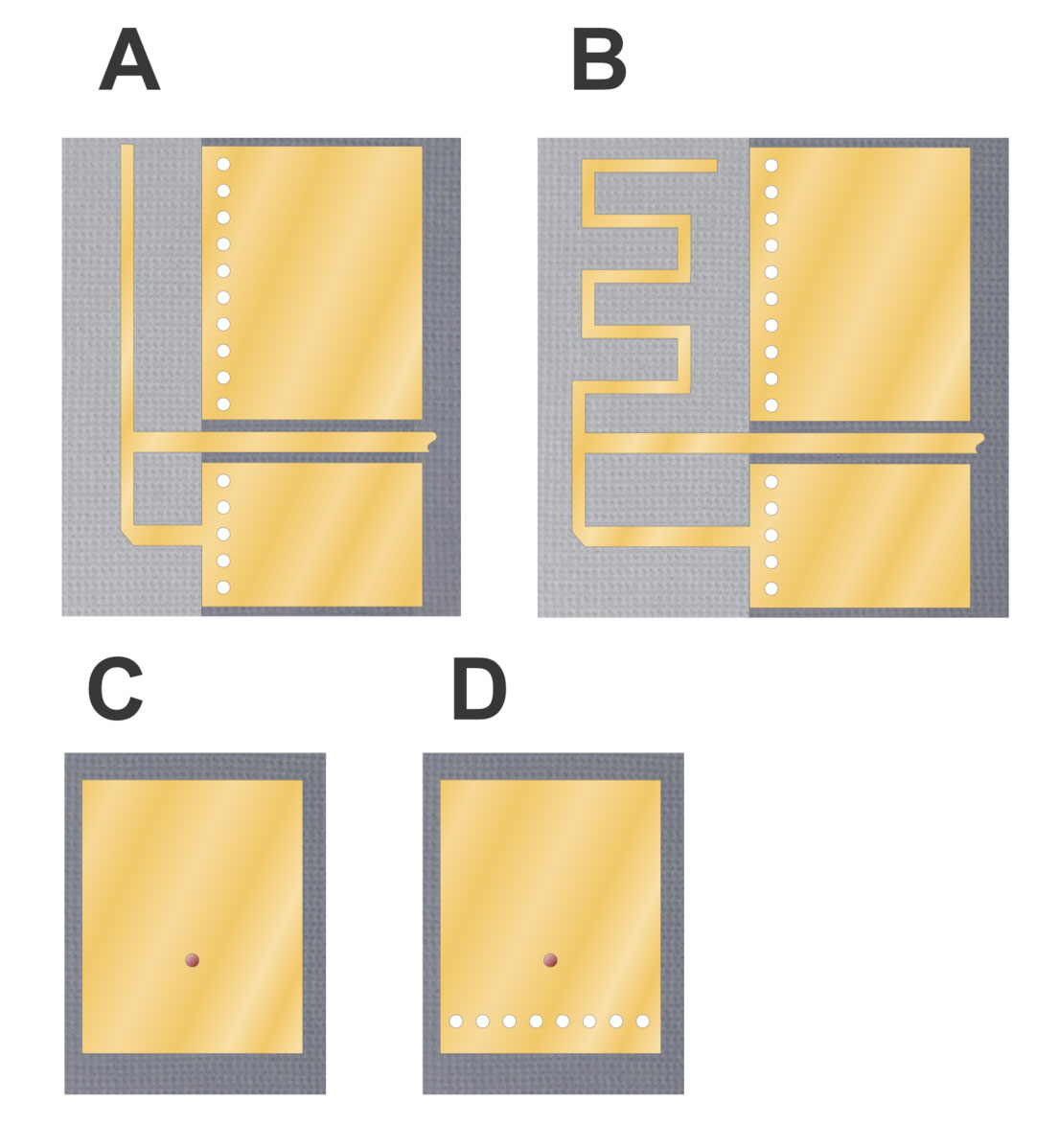
Different types of PCB antennas. Note the inverted F-type (IFA) and MIFA types in pictures A and B, respectively
Source: Wikimedia Commons Compared to the wire antenna, the PCB antenna type is 2D because it lies in the same place as the circuit board.
Chip Antenna
A chip antenna comes as a compact form-factor IC with a packed conductor inside. The compact size chip still provides a wireless range acceptable for BLE antenna designs.
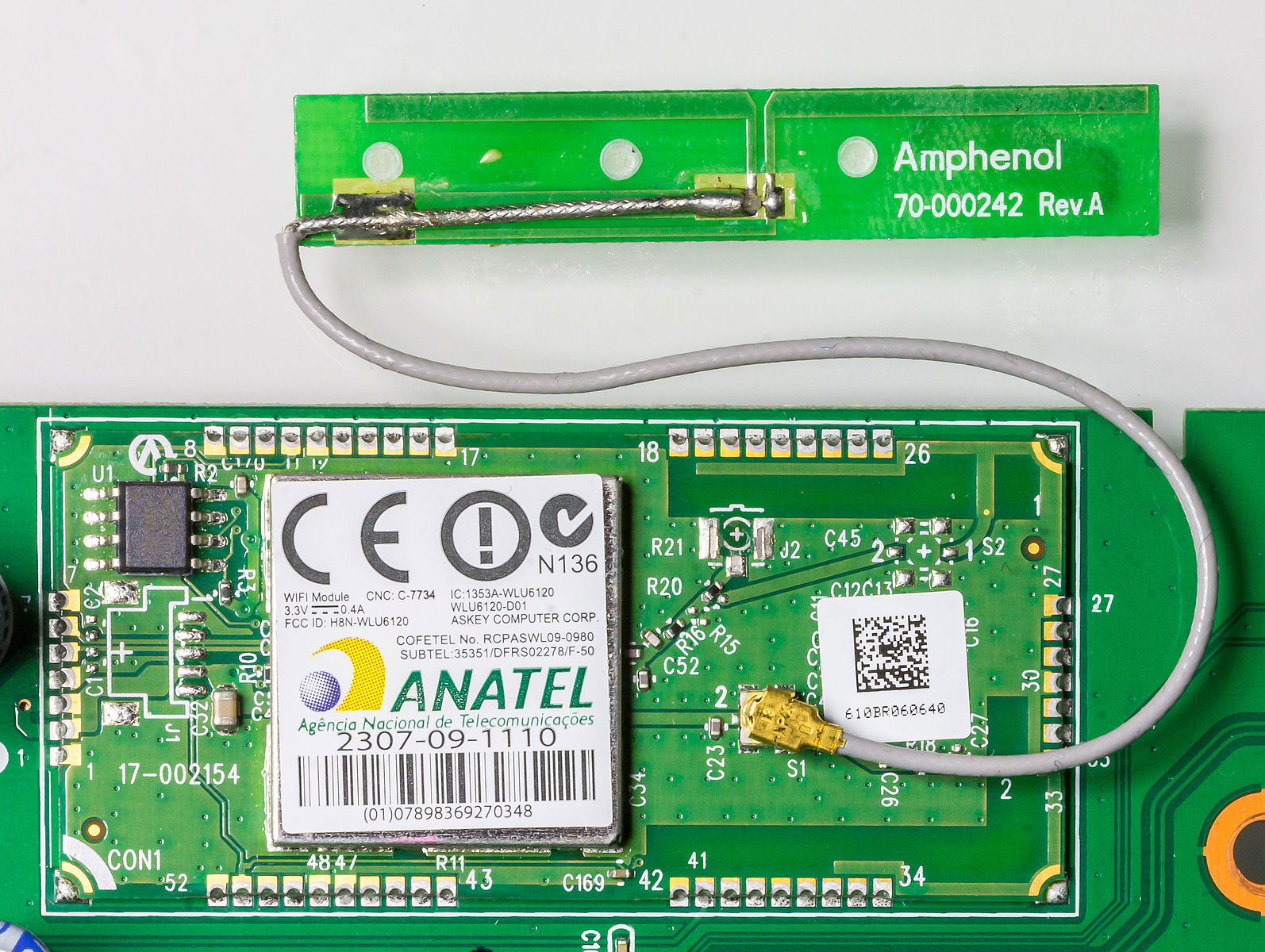
A BLE module. It contains a chip antenna
Source: Wikimedia Commons
Antenna Comparison
Since IFA and MIFA are the most common PCB trace antennas, we will compare them with the chip and wire antenna. 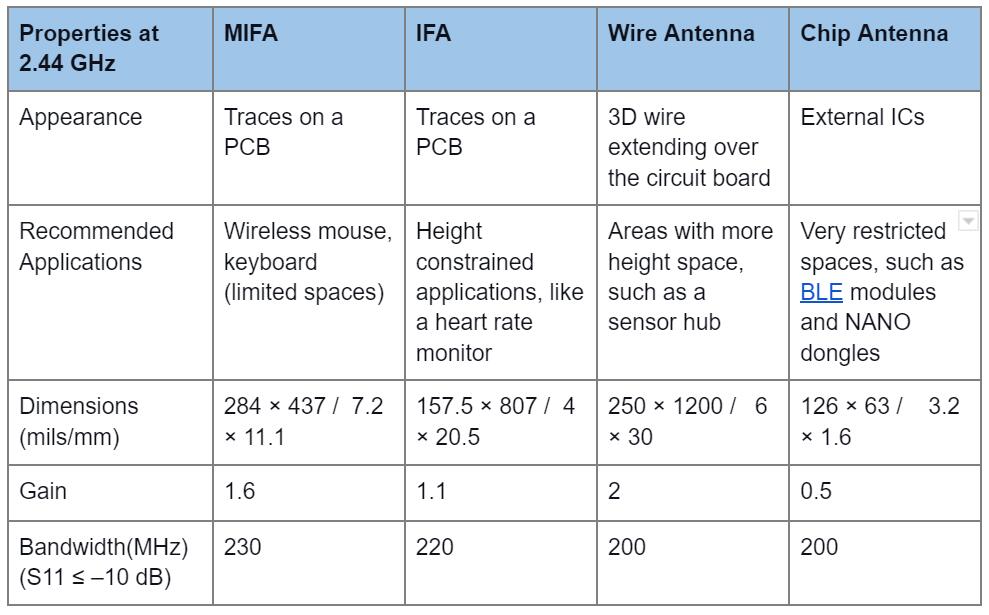
Antenna Parameters
The following are the vital performance parameters for antennas.
Return Loss
Return loss indicates how well the antenna matches the 50-Ω transmission line. The characteristic impedance of the transmission line is usually 50 Ω. But it could be different. However, 50 Ω is the industry standard for testing equipment and commercial antennas.
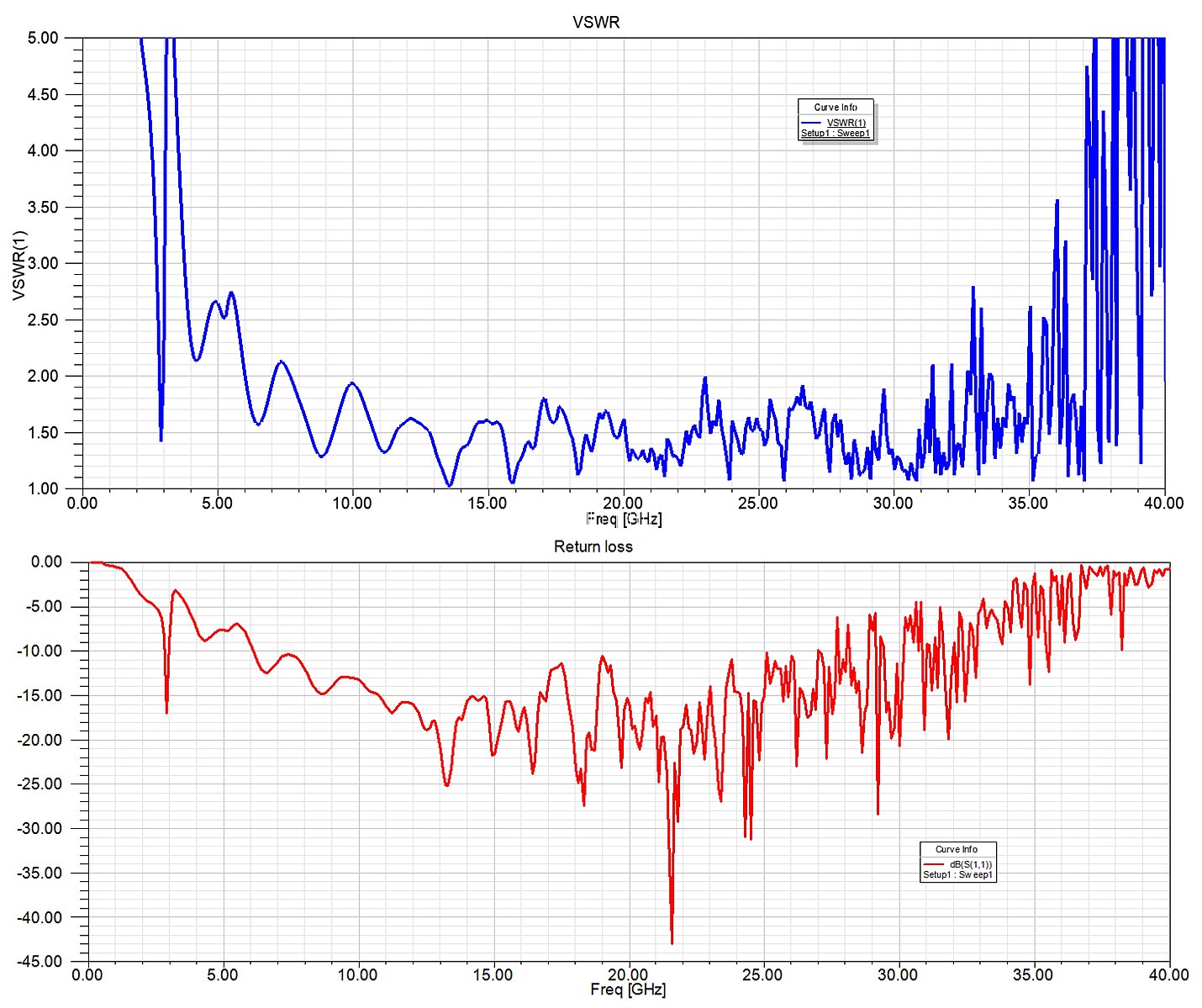
Estimated antenna bandwidth according to the return loss and VSWR schedule
Source: Wikimedia Commons
Bandwidth
Bandwidth defines the antenna's frequency response. It indicates how well the antenna matches the 50-Ω transmission line across the entire band of interest, usually 2.40 GHz to 2.48 GHz for BLE applications. A wider bandwidth is better because it reduces detuning effects coming from environmental changes surrounding the antenna.
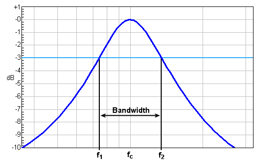
A frequency vs. gain graph showing the bandwidth range
Source: Wikimedia Commons
Radiation Efficiency
Some of the non-reflected power becomes thermal loss and gets dissipated as heat. This loss occurs due to conductor losses in the copper traces and dielectric losses in the FR4 substrate. The dissipated heat determines the radiation efficiency, whereby 100% radiation efficiency implies all non-reflected power gets dissipated into free space.
Radiation Pattern
The radiation pattern shows which directions experience more radiation and which ones experience less. This directional property helps orient the antenna optimally for its application. For instance, isotropic dipole antennas radiate equally on all sides, making them ideal for omnidirectional antenna applications. However, most antennas have a specific direction where the RF frequency signal is more powerful. A PCB antenna operates similarly and can work well as a directional antenna.
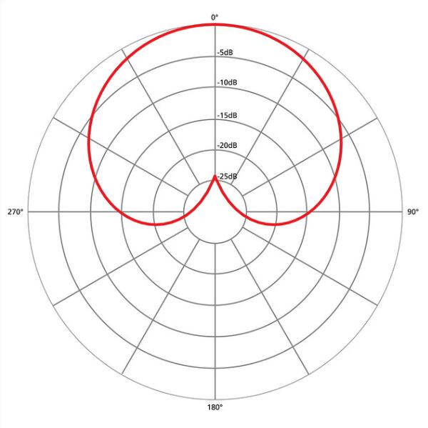
A unidirectional radiation pattern
Source: Flickr
Gain
Compared to the isotropic antenna that radiates in all directions uniformly, gain refers to the radiation on a particular side (direction of interest). dBi expresses the gain parameter by showing how strong its radiation field is relative to an ideal isotropic antenna.
How to Design a PCB Antenna
Before designing a PCB trace antenna, consider the following factors to make the design flawless.
Design Considerations
Choose the Best Type of Antenna
There are different antenna designs, with the most common ones being meandering and F-type. The standard F-type has the best trade-off between efficiency, size, and omnidirectional performance. On the other hand, meandering traces are more compact but lag in performance.
Consider the PCB Construction
A copper PCB trace length determines its resonant frequency, and the higher the frequency, the shorter the trace. Each antenna needs an area around the antenna trace with no ground fill or copper traces on any PCB layer (keep-out area). Also, wide traces give a wide bandwidth, and they can be covered using a solder mask or gold flashed. Lastly, the antenna's electrical signal performance will depend on the dielectric constant, thickness, and substrate material.
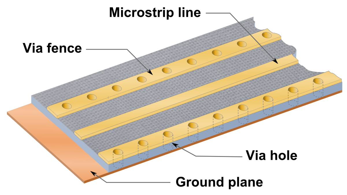
Ground Planes Are Critical
PCB antennas need a ground plane to be effective. The ground plane's size and shape will affect the antenna's performance and impedance. Therefore, it should have vias along the antenna's keep-out area edge.
A PCB ground plane
Source: Wikimedia Commons
Include Matching Components
Mismatched antennas can reduce range performance and the RF link budget. Therefore, you should place a pi-network at the antenna's feed point to avoid mismatch losses.
Impedance Matching
Besides the components, ensure the antenna and source impedance match (50 Ω) for maximum RF power transfer. Try to keep the return loss at less than or equal to -10dB
Consider the Antenna's Surrounding Environment
Metal components, enclosures, and other components can affect the radiation pattern and tuning. Therefore, ensure to keep the antenna away from metal objects, metalized plastic, or metallic enclosures.
Tune the Design for Specific Applications
Lastly, remember to tune the dimensions, matching, etc., for specific applications. Copying existing designs is not good enough because radiation patterns and gain changes as the surrounding area parameters change.
Calculations
Before going into the calculations, set these parameters straight. Select the operating frequency and substrate, then calculate the trace and substrate's length and width. Assuming the substrate material is FR4, it has a relative permeability of 4.4. We can calculate the substrate height using the following formula.
Hs is the substrate height
F is the frequency (GHz)
C is the light velocity (m/s)
Σr is the substrate's dielectric constant
As for the trace width, you can get it using the following formula:


Board and Antenna Layouts
There are two sections to consider on the circuit board. These are the antenna and crystal oscillator sections, but we will focus on the antenna section.
Design Steps
After placing the headers and connectors, fit in the U.FL connector, switch, antenna, GPIO0 switch, and microcontroller. After that, fix the antenna trace and keep in mind the trace impedance should be 50Ω. The copper trace acts as a high-frequency transmission line, and the impedance value relies heavily on the board thickness and dielectric material. Therefore, you should calculate that first, then plot the trace. You can use the impedance calculator tool to simplify your calculations. Next, calculate the trace width. Using a trace width of 70 mils, trace thickness of 1.4 mils, dielectric (board thickness) of 39.3701, and a relative dielectric constant of 4.5, we get 50 as the trace impedance. 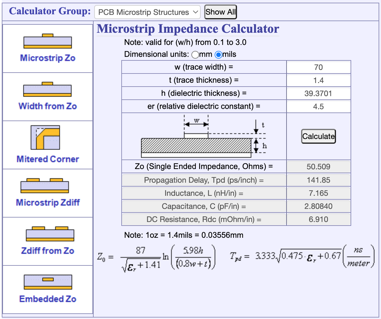
Types of Antenna Printed Circuit Boards
Yagi antenna PCB
Wheels antenna PCB
Quadcopter antenna PCB
Log period antenna PCB
Flex PCB antenna
Generic MMIC antenna PCB
Patch arrays antenna PCB
UWB antenna (Ultra Wide Band) PCB
Custom antenna PCB
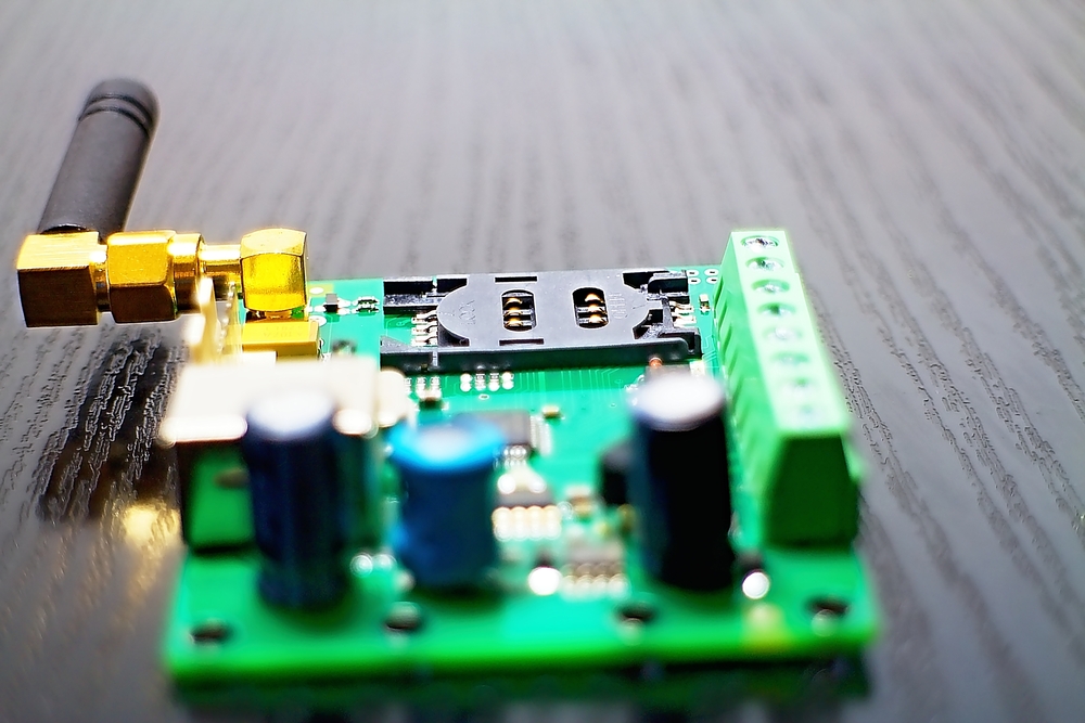
SIM card holder as part of GSM communicator with antenna
Summary
There you have it! PCB antennas are vital for modern applications, and the above design should make it easier to build one for your project. Remember to adhere to the design considerations and tune the final design to suit the specific project. If you have any questions, comments, or suggestions, don't hesitate to reach out.
Comment on this article here
-
No comment

Ripple
Hi everyone, I'm Ripple, Sales Director of KFPCBA Tech Ltd. If you are looking for a one-stop PCB and PCB assembly manufacturer in China, KFPCBA is your best choice! Please feel free to contact our team! Thanks!
Contact me now
Relevant content you may be interested in
Related articles


