


 tel:+86-18825224069
 email:
 address:201, Factory 6, Longhui Industrial Park, Fuqiao 3rd District, Xinhe Community, Fuhai Street, Baoan District, Shenzhen china
PCB Assembly Guidelines That You Need To Know Before Getting Started
Release date:2022-05-13 17:01:43 Number of views:0
If you're in the electronics industry, then there is no way that you've never heard of PCB assembly. PCB assembly is a crucial step when it comes to manufacturing electronic devices. But even as an electronic engineer, you might still be unaware of all they do and don'ts about this process.
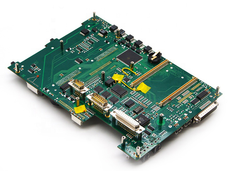
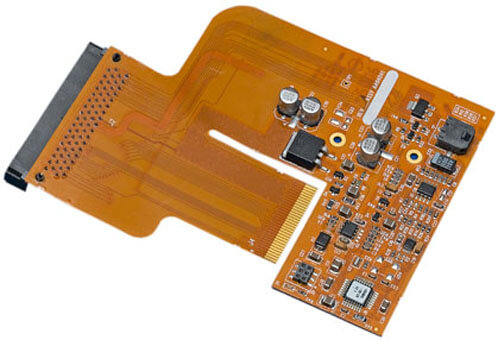
PCB is the acronym for Printed Circuit Board. This electronic circuit is made up of different parts and pieces equipped with laminated copper layers soldered together to form a circuit pattern.
These boards are used in high-end applications, like robotics, machines with motors, various scientific applications, and almost any other thing that needs a circuit board behind it. This article aims at giving you some basic PCB assembly guidelines before you get started.
To get a PCB Assembly online, there are some guidelines that you need to follow and pay attention to. Here are some of the essential policies for finding the best PCB assembly manufacturers on the internet.
What is a PCB?
A Printed Circuit Board (PCB) is a flat board with copper tracks and pads on it, used in place of discrete components like resistors, capacitors, and so on. An acid etches the PCB to form the desired pattern (most commonly) and then coated with a thin layer of plastic for protection.
It's most common for these boards to come double-sided, with copper tracks on both sides of the board, but single-sided boards are also available.
In general, PCBs are used when a particular set of components needs to be laid out in a specific way. These can be analog or digital circuits or an audio/video interface that you want to use consistently between different devices.
If you're designing a piece of hardware that includes many similar elements (like LEDs), it's often easier to have them all laid out in one PCB than to place each one individually.
What are the Different Types of Arrays?
There are many different types of arrays in PCB; some are used for spacing and some for grouping. The most common arrays are:
Spacing Arrays
The first type is spacing arrays. These are used to space out components or traces on the board. They can be measured in mils (thousandths of an inch) or picas (points).
A standard spacing array has the exact measurement on all sides of the rectangle. This is called a "constant" spacing array, and you will find it in almost every design file.
Grouping Arrays
The second type of array is a grouping array, which allows you to group individual components or traces into one object that can be easily moved around as a single entity.
These are often used for things like connectors or LEDs, where there may be several of them close to each other that need to be kept together when moving them around on the board layout.
Grid Array
This type of array is used for ICs having multiple pins. It is used for BGA devices or dense pitch QFP devices. The pins are arranged in rows and columns with a pitch equal to half the distance between two adjacent pins.
This array provides better thermal dissipation than the other arrays because it has a greater heat sink area. More airflow can pass through it without interference from other components on the board.
Resistor Array or Resistor Network
A resistor array is an arrangement of resistors in parallel or series. It can be used as a low-cost alternative to individual resistors.
The advantage of using resistor arrays is that they reduce the number of parts needed for the design and save you money on manufacturing costs by allowing you to reuse the same piece repeatedly. Resistors have a very high tolerance, so they don't have to be matched within 5% or 10%.
Single-Level Arrays
These are simple arrays with only one level of hierarchy. They use the same number of layers as the original component and typically require no additional artwork.
Multi-Level Arrays
These are more complex and have multiple levels of hierarchy. They often require additional artwork to ensure that each element in the array looks correct on the layer it is drawn on.

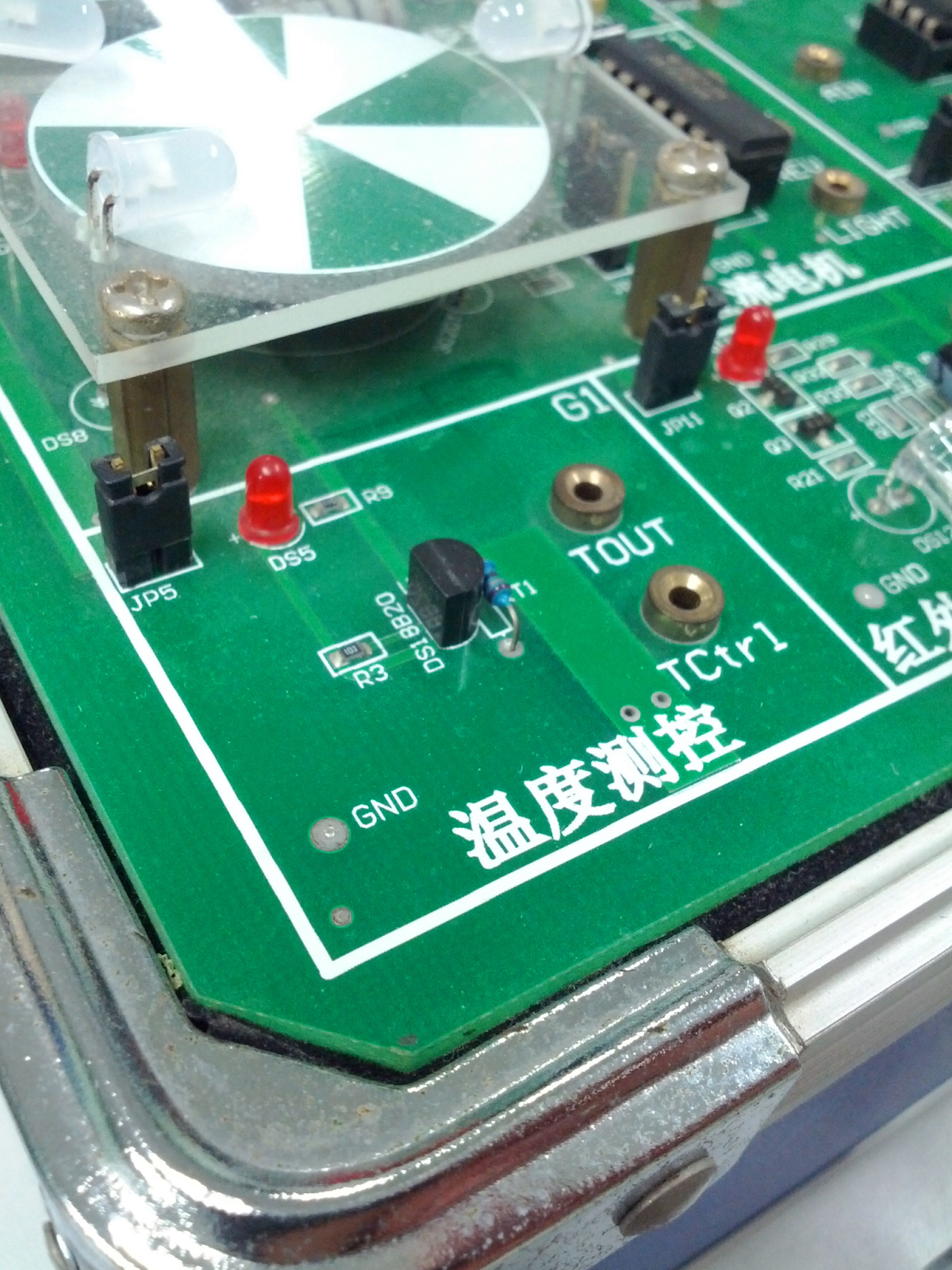
What Are The Important Steps In PCB Assembly?
Soldering
The soldering process is the essential step in PCB assembly. It involves connecting components to the board by melting a tin-lead alloy, called solder, with a soldering iron or gun. The solder used in PCB manufacturing is typically between 63 and 40 percent tin and 37 to 63 percent lead.
To ensure that a good solder joint is formed, several things must be done correctly:
The parts must fit together correctly and be held in place during the soldering process.
The flux should be removed from around the joint (wetted) so that when it melts, it does not flow into unwanted places or interfere with the proper wetting of other areas of the joint.
A good quality solder must be used; this ensures no voids (blobs), which could cause an incomplete joint or even fail.
Only high-quality fluxes should be used; they help remove oxides from around joints and allow them to wet more easily and quickly during soldering operations.
Drilling
Drilling is one of the essential steps in PCB assembly because it allows for the proper insertion of components onto the board. The holes must be drilled at exact locations corresponding to the placement marks made on the PCB during fabrication.
Drill bits have different diameters, so choosing a drill bit that matches the size of your components is crucial to successful drilling.
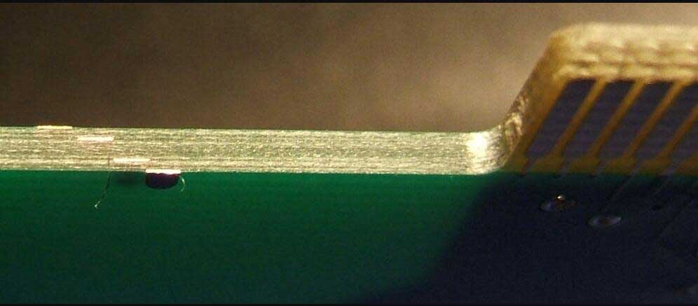
Plating
This process adds solderability to different surfaces like tin-lead plating, nickel plating, gold plating, etc. In this process, an electroplating machine can be used, which has a set of electrodes at its base through which current passes, which then attaches metal ions on the surface of the object being processed (e.g., PCB).
Routing
Routing involves cutting traces on a PCB board for electrical connections between various components on the board. Routes are usually cut with a router, but they can also be cut by hand with a pair of wire strippers or scissors (though this is not recommended).
Silkscreen Printing
Silkscreen printing is a method of applying labels to electronic devices and printed circuit boards (PCBs). The application method involves placing a thin layer of ink onto a substrate, then applying pressure to transfer it from the donor roll to the receiving surface.
This process can be done manually or with automated equipment, depending on volume requirements and the complexity of design requirements.
Inspection
The next step in the PCB assembly process is inspection. This involves checking whether all components have been installed correctly and whether any non-working parts are on the board. The inspector can use an optical microscope or a magnifying glass to check for quality issues such as missing solder joints or incorrect component placement.
How to Select Components for PCB Assembly?
PCB Material
The most crucial factor to consider when selecting your PCB material is the type of application. Some materials are better suited for high-frequency applications, while others are more durable and can withstand harsher environments.
If you're not sure what type of board you need, consult with an engineer or manufacturer to determine which material is best suited for your product.
A good rule of thumb is that materials with higher dielectric constants (Dk) are better suited for high-frequency applications. In contrast, materials with lower Dk are more durable and can withstand harsh environments.
Mandrel Plating
Mandrel plating is an effective solution for the PCB assembly. It involves the process of electroplating copper on the surface of a printed circuit board. This process improves the final product's quality and increases its durability.
The advantage of mandrel plating is that it helps prevent oxidation on your PCBs' surface. It also prevents corrosion, making it a perfect option for use in various industries such as defense, medical, and aerospace.
Holes
Holes are one of the most critical components that need to be considered while manufacturing PCBs because they help connect different parts.
They play an essential role in ensuring the functionality and performance of your PCBs even after years of use. Therefore, you should always make sure that you choose appropriately sized holes for your PCBs to carry out their functions efficiently with ease.
Bottom Line
Assembly is the time-consuming process of putting a PCB into a case. No matter the size of your PCB, whether it's primary or complex, preparation and planning are critical to an efficient assembly process.
We've put together a set of best practices that address common assembly issues to aid designers and assemblers. These tips should help make your next PCB assembly project run more smoothly.
Many people are more comfortable with a soldering iron than a screwdriver, but assembling circuit boards via surface mount technology (SMT) is still an intimidating prospect to most.
However, the ideas and guidelines mentioned above apply whether you use SMT or through-hole methods. So it can be done once by someone such as yourself, it'll be even more accessible on the next project.
Hopefully, putting together a prototype board will feel less like rocket science the next time you get started. Taking the time to plan can save you from countless headaches and delays down the road, so keep these guidelines in mind and consider best practices for every stage of your project.
Comment on this article here
-
No comment

Ripple
Hi everyone, I'm Ripple, Sales Director of KFPCBA Tech Ltd. If you are looking for a one-stop PCB and PCB assembly manufacturer in China, KFPCBA is your best choice! Please feel free to contact our team! Thanks!
Contact me now


