



 tel:+86-18825224069
 email:
 address:201, Factory 6, Longhui Industrial Park, Fuqiao 3rd District, Xinhe Community, Fuhai Street, Baoan District, Shenzhen china
The Complete DFM Checklist for PCB Designers
Release date:2026-11-20 09:00:00 Number of views:0
Quick answer: Design for manufacturability (DFM) means designing your PCB so a factory can build it right the first time, at volume, without heroics. A proper DFM review covers seven areas — board outline, drill and via rules, copper spacing, solder mask and silkscreen, panelization, component placement, and test access — and catching a violation at design time costs minutes instead of a $5,000 scrap run. The fastest way to validate your design is a free DFM review from your manufacturer before you order; start with a detailed PCBA quote that includes engineering review.
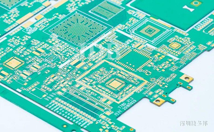
This is the complete DFM checklist our engineers apply to every incoming design — use it before you send your next board out.
1. Board Outline and Mechanical
- Outline on a dedicated mechanical layer, with dimensions and tolerances — not just "the edge of the copper."
- Minimum internal corner radius of 0.5–1 mm or routed reliefs; sharp internal corners concentrate stress and crack the board during depaneling.
- Keep-outs for connectors, mounting hardware, and enclosure rails clearly marked, with 0.3 mm+ clearance from copper to board edge.
- Board thickness matched to the stack-up (1.0/1.6/2.0 mm are the cheapest and most reliable standards); note thickness tolerance for press-fit connectors.
- Edge plating or castellated holes specified explicitly if the board mates with a card edge or module footprint.
2. Drill and Via Rules
- Finished hole size ≥ 0.2 mm (8 mil); below this, drill breakage and plating voids rise sharply in cost and risk.
- Annular ring ≥ 0.05 mm (prefer 0.1 mm) so drill misalignment never breaks out of the pad.
- Via-to-via and via-to-trace spacing ≥ 0.15 mm for standard processes.
- Aspect ratio ≤ 10:1 for reliable plating (board thickness ÷ drill diameter).
- Filled and capped vias only where the package demands them (fine-pitch BGAs) — they add real cost.
- Specify tented vias (solder mask over unused vias) to prevent paste scavenging during reflow.
3. Copper, Spacing, and Impedance
- Line/space ≥ 4/4 mil for standard 1 oz copper; 3/3 mil is possible at a premium; below that, expect yield loss.
- Copper balance across each layer: large unbalanced copper areas cause board warp during lamination. Add thieving/hatching to sparse layers.
- Impedance requirements stated per layer with target values and tolerances (±10% is standard), and a controlled dielectric distance in the stack-up.
- Copper-to-board-edge ≥ 0.3 mm; routing copper to the routed edge risks shorts after depaneling.
- Thermal relief on plane connections to pads that must be soldered — direct plane ties make hand and rework soldering miserable.
4. Solder Mask, Silkscreen, and Surface Finish
- Solder mask dam ≥ 3 mil (0.075 mm) between fine-pitch pads; below this, mask slivers lift and cause shorts.
- Pad coverage: mask-defined pads on fine-pitch parts where the fabricator recommends it; otherwise copper-defined with proper dam.
- Silkscreen readable and non-overlapping: reference designators ≥ 0.8 mm high, never printed over pads or vias.
- Surface finish choice stated: ENIG for fine pitch and shelf life, HASL for cost, OSP for volume with short storage windows.
- Peelable mask or carbon ink areas identified if used (keypads, edge contacts).
5. Panelization and Depaneling
- Panel size optimized for the fabricator's standard panel (e.g., 18"×24") with 5–10 mm rails and tooling strips for fiducials and bad marks.
- Depaneling method chosen early: V-score for straight-edged rectangles with 0.3 mm+ spacing; routed (tab-routed) panels with mouse bites or breakaway tabs for anything else. Never mix thin traces near score lines.
- Components ≥ 5 mm from the panel edge (and from V-score lines) to survive depaneling stress.
- Fiducials: 1 mm solid circles with 2–3 mm mask clearance on the panel rails, plus board-level fiducials for fine-pitch placement.
- Breakaway tab placement reviewed so removal never leaves burrs near connectors or RF shields.
6. Component Placement and Assembly DFM
- One clear polarity convention — all diodes, LEDs, electrolytics oriented the same way; ambiguous silkscreen polarity is a top cause of wrong-way assembly.
- Spacing for rework: ≥ 1 mm between adjacent components where a hot-air nozzle needs access; larger around BGA, QFN, and connectors.
- Heavier components on the reflow-pass side per the assembly plan; tall parts placed where they won't shadow fine-pitch printing.
- No components in test point "shadows" — keep probes reachable.
- Fiducial and tooling hole compatibility with the assembly house's conveyor and clamping system.
7. Test Access and Documentation
- Test points for every net you intend to probe: ≥ 0.9 mm diameter, ≥ 2.54 mm grid, with unobstructed top or bottom access.
- ICT access or flying-probe friendly layout — don't seal everything under shields without test ports.
- Complete documentation package: Gerber (RS-274X, one file per layer), NC drill, IPC-D-356 netlist (invaluable for catching design errors the eye misses), pick-and-place file, and a readable assembly drawing.
- Revision and version marking in copper or silkscreen — traceability is a DFM requirement, not a nicety.
Special DFM Rules for HDI and Fine-Pitch Designs
Once your design moves beyond standard technology, additional rules apply on top of the checklist above:
- Microvias (laser-drilled ≤ 0.15 mm): stack them no more than two high, or use staggered vias to avoid reliability traps; specify filled and planarized microvias for pad-on-via designs.
- 0.4 mm-pitch BGAs and below: require via-in-pad with filling, and ENIG surface finish — HASL's uneven surface will bridge these pads during printing.
- 0201 and 01005 passives: keep them off the reflow-first side; their small thermal mass tombstones easily when neighboring parts are still heating.
- High-layer-count boards (12+): specify sequential lamination explicitly, review resin fill percentages on buried vias, and require cross-section reports on first articles.
- Controlled impedance on HDI: the effective dielectric distance to an adjacent plane changes near microvias — flag impedance-critical traces so the fabricator adjusts locally or routes around.
Fine-pitch DFM is where fabricator choice matters most: a shop that builds HDI daily will catch these in CAM review; one that builds it monthly will build your board wrong with total confidence.
The DFM Review Meeting: What a Good Fabricator Actually Checks
A serious DFM review is not an automated "DFM tool passed" checkbox. An engineer looks at your stack-up against your impedance claims, your copper balance against your board thickness, your fiducial scheme against your fine-pitch parts, and your panel drawing against your depaneling method — then sends back a written report of violations ranked by severity. At our factory this review is free and standard on every order; it typically returns within one working day alongside your manufacturing and assembly quotation.
Automated DFM Tools vs Engineering Review
Most fabricators run automated DFM software (Valor, Ucamco, or in-house CAM rule checks) on every job. These tools are excellent at geometric violations — spacing, annular ring, mask dams — and every design should pass them. But they cannot judge design intent: whether your fiducial placement matches your fine-pitch components, whether your panelization method will crack a 0.8 mm board, or whether your test-point layout is actually reachable with a flying probe. Those judgments require an engineer reading your design goals against your files. The practical rule: automated DFM catches rule violations; human DFM review catches design mistakes. You need both, and any factory quoting without offering the second is selling you machine time, not engineering.
The Cost of Skipping DFM
| Defect found at | Typical cost to fix |
|---|---|
| Design review (before order) | Minutes of layout time |
| Fabrication (cam review) | Days of delay; $100–500 in engineering changes |
| First article / prototype | $500–5,000 scrap + 1–2 weeks |
| Volume production | $10,000+ scrap, line downtime, missed market windows |
| Field (after shipment) | Warranty, recalls, reputation — unbounded |
When Your Fabricator Flags a Violation: How to Respond
A DFM report is a negotiation input, not a verdict. Handle it in three passes:
Pass 1 — Fix unconditionally: violations that break the laws of physics or process capability — holes below minimum drill, annular ring under 0.05 mm, mask dams under 3 mil. Change the design; there is no alternative build.
Pass 2 — Fix or pay consciously: items the fabricator can build at reduced yield or premium cost — 3/3 mil routing on a standard process, heavy copper on fine pitch, tight positional tolerances. Ask for the quoted yield impact in writing, then decide whether the electrical benefit justifies the premium or a redesign is cheaper.
Pass 3 — Push back with data: items where the fabricator is applying conservative generic rules rather than your board's actual constraints. Example: a fabricator citing "standard" impedance stack-ups when your simulation used a different dielectric, or defaulting to a thicker minimum dielectric than your voltage spacing requires. Answer with your calculated values — dielectric withstand voltage, insertion loss budget, crosstalk margins — and request a deviation approval signed by their engineering manager. Real factories accommodate documented deviations every day; the conversation also tells you whether you are dealing with engineers or order-takers.
Whatever you decide, capture the resolution in the fabrication notes of your next revision so the CAM engineer never has to ask twice. DFM is a living document: every production order teaches something that belongs in your design rules file.
FAQ
What files does a DFM review need?
Gerbers, NC drill files, the IPC-D-356 netlist, board stack-up, and ideally the pick-and-place file and assembly drawing. The netlist in particular lets the fabricator verify your copper matches your intended connectivity.
Is DFM different for prototypes vs production?
The rules are the same, but the stakes differ: a prototype run forgives a lot because a human can babysit it. Production cannot. If a design will ever go to volume, review it against production DFM rules from day one — retrofitting manufacturability later means re-laying out the board.
What is the most common DFM violation you see?
Insufficient annular ring on vias and copper routed too close to the board edge. Both are invisible in the CAD view, and both cause real failures — broken plating and edge shorts — that only appear after fabrication or depaneling.
Do I need DFM if I use a standard process like JLC's 4-layer stack-up?
Standard stack-ups remove some DFM risk (impedance and lamination are pre-engineered), but they say nothing about your routing, spacing, panelization, or assembly access. DFM review is still required — it just goes faster.
Comment on this article here
-
No comment

Ripple
Hi everyone, I'm Ripple, Sales Director of KFPCBA Tech Ltd. If you are looking for a one-stop PCB and PCB assembly manufacturer in China, KFPCBA is your best choice! Please feel free to contact our team! Thanks!
Contact me now
Relevant content you may be interested in
Related articles