


 tel:+86-18825224069
 email:
 address:201, Factory 6, Longhui Industrial Park, Fuqiao 3rd District, Xinhe Community, Fuhai Street, Baoan District, Shenzhen china
The Specific Process Of 8-layer PCB Proofing And Ordinary Circuit Board Proofing
Release date:2022-11-23 16:05:33 Number of views:117
The specific process of 8-layer PCB proofing and ordinary circuit board proofing
The general process of 8-layer pcb proofing is similar to that of ordinary circuit boards, but there are more pressing processes than ordinary circuit boards. Today, the editor will take you to see what is the specific process of 8-layer PCB proofing production?
A brief description of the differences between ordinary double-sided PCB boards and multi-layer PCB boards:
The double-sided board is a medium layer in the middle, and both sides are wiring layers. A multi-layer board is a multi-layer wiring layer. There is a dielectric layer between every two layers. The dielectric layer can be made very thin. A multilayer circuit board has at least three conductive layers, two of which are on the outer surface, while the remaining layer is synthesized inside the insulating board. The electrical connections between them are usually made through plated through holes in the cross-section of the board.
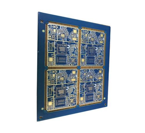
The manufacturing process of 8-layer pcb proofing is the same as the manufacturing process of pcb multi-layer board, let's see what processes are there.
1. 8-layer pcb proofing production - the purpose of blackening and browning
①Remove surface oil, impurities and other pollutants;
② Increase the specific surface of the copper foil, thereby increasing the contact area with the resin, which is conducive to the full diffusion of the resin and the formation of a greater bonding force;
③ Make the non-polar copper surface become the surface with polar CuO and Cu2O, and increase the polar bonding between copper foil and resin;
④The oxidized surface is not affected by moisture at high temperature, reducing the chance of delamination between copper foil and resin.
⑤The boards with the inner circuit must be blackened or browned before they can be laminated. It is to oxidize the copper surface of the inner board. Generally, the generated Cu2O is red and CuO is black, so Cu2O in the oxide layer is mainly called browning, and CuO is mainly called blackening.
1. Lamination is the process of bonding each layer of circuits into a whole with the help of B-stage prepreg. This bonding is achieved through interdiffusion and penetration of macromolecules on the interface, and then interweaving. The process of bonding the various layers of circuits into a whole with a prepreg. This bonding is achieved through interdiffusion and penetration of macromolecules on the interface, and then interweaving.
2. Purpose: To press discrete multi-layer boards together with bonding sheets to form multi-layer boards with the required number of layers and thickness.
① Typesetting Design the copper foil 8-layer circuit board , adhesive sheet (prepreg), inner layer board, stainless steel, isolation board, kraft paper, outer layer steel plate and other materials and stack them according to the process requirements. If the board has more than six layers, pre-typesetting is required. Copper foil, adhesive sheet (prepreg), inner layer board, stainless steel, isolation board, kraft paper, outer layer steel plate and other materials are laminated according to the process requirements. If the board has more than six layers, pre-typesetting is required.
② Lamination process Send the stacked circuit board into the vacuum heat press. Using the heat energy provided by the machine, the resin in the resin sheet is melted to bond the substrate and fill the gap.
③ Lamination For designers, the first thing to consider in lamination is symmetry. Because the board will be affected by pressure and temperature during the lamination process, there will still be stress in the board after the lamination is completed. Therefore, if the two sides of the laminated board are uneven, the stress on the two sides will be different, causing the board to bend to one side, which greatly affects the performance of the PCB. Keyou Circuit specializes in the production of high-precision multi-layer circuit boards. The products are widely used in: LCD liquid crystal modules, communication equipment, instruments and meters, industrial power supplies, digital, medical electronics, industrial control equipment, LED modules/modules, electric energy, transportation, Science and education research and development, automobile, aerospace and other high-tech fields. In addition, even on the same plane, if the distribution of copper is uneven, the flow rate of the resin at each point will be different, so that the thickness of the place with less copper will be slightly thinner, and the thickness of the place with more copper will be slightly thicker. Some. In order to avoid these problems, factors such as the uniformity of copper distribution, the symmetry of the stack, the design and layout of blind buried holes, etc. must be carefully considered during the design.
2. 8-layer pcb proofing production - desmearing and sinking copper
Purpose: To metallize through-holes.
①The base material of the circuit board is composed of copper foil, glass fiber and epoxy resin. In the production process, the section of the hole wall after the substrate is drilled is composed of the above three parts of the material.
② Hole metallization is to solve the problem of covering the section with a uniform layer of metal copper that is resistant to thermal shock. Hole metallization is to solve the problem of covering the section with a uniform layer of metal copper that is resistant to thermal shock.
③The process is divided into three parts: 1. Decontamination process, 2. Electroless copper deposition process, 3. Thickened copper process (full board electroplating copper).
Three, 8-layer pcb proofing production - sinking copper and thickened copper
Hole metallization involves a concept of capability, thickness-to-diameter ratio. The aspect ratio refers to the ratio of the plate thickness to the hole diameter. , thickness-to-diameter ratio. The aspect ratio refers to the ratio of the plate thickness to the hole diameter. When the board gets thicker and the hole diameter keeps decreasing, it becomes more and more difficult for the chemical yao water to enter the depth of the drill hole. Although the electroplating equipment uses vibration, pressure, etc. to allow the yao water to enter the center of the drill hole, the concentration difference caused Thin center plating is still unavoidable. At this time, there will be a slight open circuit phenomenon in the drilling layer. When the voltage increases and the board is impacted under various harsh conditions, the defects are completely exposed, causing the circuit of the board to be disconnected, and the specified work cannot be completed.
Therefore, designers need to know the process capabilities of board manufacturers in a timely manner, otherwise the designed PCB will be difficult to realize in production. It should be noted that the parameter of thickness-to-diameter ratio must be considered not only in the design of through holes, but also in the design of blind buried holes.
Four, 8-layer pcb proofing production - outer layer dry film and graphic plating
The principle of the outer layer graphics transfer is similar to that of the inner layer graphics transfer. They both use photosensitive dry film and photographing to print the circuit graphics on the board. The difference between the outer dry film and the inner dry film is:
① If the subtraction method is used, the outer dry film is the same as the inner dry film, and the negative film is used as the board. The part of the cured dry film on the board is the circuit. The uncured film is removed, and the film is retreated after acid etching, and the circuit pattern is left on the board because of the protection of the film.
For more questions about PCB multi-layer boards such as 8-layer PCB proofing and production, you can consult Jinruixin Special Circuit. Jinruixin Special Circuit has more than ten years of industry production experience, and can realize rapid proofing and small and medium-sized batch production of 2-30-layer circuit boards. The team has 300 people Professional manufacturing, strict quality control in every link to ensure product performance.
Comment on this article here
-
No comment

Ripple
Hi everyone, I'm Ripple, Sales Director of KFPCBA Tech Ltd. If you are looking for a one-stop PCB and PCB assembly manufacturer in China, KFPCBA is your best choice! Please feel free to contact our team! Thanks!
Contact me now
Relevant content you may be interested in
Related articles


