


 tel:+86-18825224069
 email:
 address:201, Factory 6, Longhui Industrial Park, Fuqiao 3rd District, Xinhe Community, Fuhai Street, Baoan District, Shenzhen china
A Complete Guide on How to print pcb board
Release date:2022-08-17 10:07:20 Number of views:0
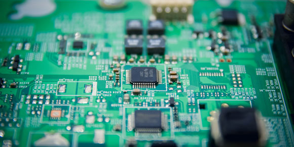
PCB stands for printed circuit boards and has revolutionized the world of electronics since they entered the market. Not only do PCBs help you convert your temporary circuit made on breadboard into a permanent one, but they also make it look neat and professional.
In addition, previously PCBs were only capable of accommodating through hole or TH electrical components. However, as the technology progressed, and the need for PCBs became crucial for almost all electrical circuits, whether small or large, PCBs on which SMD can be soldered were introduced.
With that said, whether you want a PCB for SMD or TH components, the PCB itself goes through several fabrication steps before it is ready. Moreover, many novices in the field of electronics search for how to print PCBs.

Steps on how you can print a PCB you need to know about
Before discussing what are some of the PCB printing steps, you must know what are some basic steps that go into PCB manufacturing. It is worth mentioning that some of these steps are better to be left to professionals as one mistake can cause your PCB to malfunction. However, some are completely ok and can be done by a beginner as well.
Step 1: Create your electrical design/schematic
The first step before you can know how to print PCBs is creating a design or a schematic. In layman’s terms, a schematic is an electrical drawing consisting of several electrical or electronics components connected for single or multipurpose. Initially, all PCBs are designed through PCB software, such as Eagle, EasyEDA, Altium, and more.
Make sure you know what type of PCB design are you making and what would its function be. Knowing things like these would help you know about the right electrical/electronic components, which would save your time.
There is software in which you can directly make a PCB layout or a schematic while others have the functionality of converting your design into a layout. Check out the features of the software you would be used to create your PCB design.
Step 2: Design check
After converting your design into a PCB layout, make sure you check your design completely and also view the model in 3D. Some of the things you should check before printing out your created design are:
Width and position of the electrical pads. Pads are the area on the PCB on which you would be soldering surface-mount or through hole components.
Routing the traces and or electrical components. Routing means setting the position of traces that connect with other electrical components. Most PCB designing software offers the auto-routing tool that automatically determines the ideal position of each active element you would be soldering on your PCB.
Adjusting the width of electrical traces (conducting copper lines). Some traces after creating your schematic would be thin or thick. However, make sure that the traces connecting relatively large electrical components, such as ICs, are a bit thick, otherwise, these components would not receive optimal operating voltage.
Step 3: Printing the PCB
After completing the schematic, the next step is to print the PCB. To print the PCB, you need to have certain things like:
Butter paper, or a toner, preferably A4 size
One-sided copper plate/laminate board
Inkjet printer
After gathering the required things, make sure to follow the steps listed below:
Take out the print of your layout
This step seems a no-brainer, but many beginner PCB designers get confused about what should they do after successfully creating the design. Most PCB design software has two options, such as Save as PDF, and the other is to export the Gerber File. If you are printing the PCB on your own, forget the Gerber File option for now.
Click the Save as PDF option, or if your PCB design software has an option like save PCB as an image or likewise, click that and you would have downloaded your PCB layout. After this, take out the butter paper, insert it into your inkjet printer, and print the layout on the butter paper. Make sure to print the layout on the shiny/glossy side of the butter or transfer paper.
Resize the image
After successfully taking out the print, make sure to resize the print so that it can be easily transferred to the copper board/laminate board leaving enough space on it. In addition, make sure that the laminate board is also according to the size of your layout, so the circuit would look more professional.
Remove the copper from your laminate board
The third step that includes how to print PCBs is to remove the integrated layer of the copper or resist from one side of the laminate board or copper board. To remove the excess copper from the one-sided laminate board, take a scrub and rub off the copper. You can also use an alkaline solution to remove the unwanted copper and hardened photoresist.
Why you should remove the copper from the board?
The primary reason you should remove the copper or the resist from the board is that excess copper hinders the printed image. Therefore, if the image of your layout would not visible on the board, it would cause numerous inconveniences while etching.
Step 4: Transfer the PCB layout to the laminate
The next step includes transferring the layout on the copper board. To do this, take out your resized PCB print and flip the top layer horizontally (only do this if you didn’t print the mirrored image of your layout).
Then place the image onto the board (laminate side), and press it with a hot iron for about 10 minutes. Make sure the iron is not too hot, and the pressure you are applying is not too much as well as it can burn the paper or break your board.
Step 5: Masking or covering the copper traces
After transferring the PCB layout to the board, there is a chance you might encounter a scenario where the traces of your design would be weak or incomplete (not transferred onto the board perfectly).
To fix this grab a permanent marker and draw the incomplete lines. This process is also known as the masking process.
Step 6: Plate etching process
This step needs to be done with a lot of practice and focus. Make sure to first wear protective gloves so that you do not hurt yourself. Next thing is to get a leftover newspaper at the bottom so it keeps the floor very clean. Then take the solution of the etching and place it carefully down. To dissolve the ferric chloride powder in the water a plastic box can come in handy and easy to do the job.
For about 30 minutes you would have to keep the printed circuit board in the prepared solution of the ferric chloride. The removal of the excess copper begins once the ferric chloride starts to react with the unmasked copper type.
This whole process of etching is termed the etching of the printed circuit board. However, you need to be careful when you are taking the printed circuit board from the prepared solution with the help of pliers. If for some reason the etching is not done properly then let it soak up in the solution for some more time.
Things to do after the printing of the printed circuit board
When you have properly learned how to print pcb and all the steps; the next few things after how to print pcb need to be determined as well.
Like, drilling is necessary that is done with the help of a pcb drilling machine. This helps to keep the printed circuit board safe and secure. Drilling is often based upon the components present in the printed circuit board.
Pcb plating is also a crucial factor that should be done after learning how to print pcb. This step includes the pcb board to be covered with the help of a micron thick layer. This layer is usually well placed between the holes that you drilled.
The final etching step is also known to be essential while you have learned how to print pcb with proper guidelines.
This helps in the elimination of excessive copper and makes the connections of the printed circuit board even stronger. With the help of this step, you can easily be certain that the printed circuit board is very much ready for the soldering process.
Then comes the step of the soldering mask which is deemed a useful step. Here, a solder mask covers the printed circuit board and then goes through the process of the ultraviolet ray exposure process. This helps in the strengthening of the printed circuit board.
Conclusion
How to print a pcb is no longer an unanswered question. With the help of the right guidance and steps, you can easily learn how to print a pcb even if you lack experience or are not quite sure of how to start with the whole process. Hence, if you are worried then we have got you covered.
Comment on this article here
-
No comment

Ripple
Hi everyone, I'm Ripple, Sales Director of KFPCBA Tech Ltd. If you are looking for a one-stop PCB and PCB assembly manufacturer in China, KFPCBA is your best choice! Please feel free to contact our team! Thanks!
Contact me now
Relevant content you may be interested in
Related articles


