


 tel:+86-18825224069
 email:
 address:201, Factory 6, Longhui Industrial Park, Fuqiao 3rd District, Xinhe Community, Fuhai Street, Baoan District, Shenzhen china
how to read a circuit board(pcb) Layout schematic ,Step by Step Guide 2022
Release date:2022-08-19 10:56:22 Number of views:0
Reading PCB layout refers to the rules for the layout of electronic elements on a printed circuit board. When designing an electronic circuit on a printed circuit board, it is important that you have a clear plan and detailed instructions on what you can and cannot do before you start the PCB layout.

PCB Layout | Initial steps
Understanding the circuit is critical to the design, such as knowing the maximum current and voltage that will flow in the circuit of each conductor. Knowing these values, it will be easier for you to determine the track width and the type of PCB that will be used.
The voltage difference between each track determines the required clearance between each conductor. If there is not enough clearance, there is a chance that the electrical potential between each track will cause sparking and shorting of the PCB. Therefore, it is very important to follow some of these basic requirements before proceeding with PCB design.
If you don't consider important aspects when doing PCB design and layout of electronic components, you may end up with a design that doesn't work well. Inadequate wiring can lead to problems such as EMI, component conflicts on either side of the board, the limited functionality of the circuit, and even circuit failure.
In addition, if the wiring does not work the first time, it will have to be redone, which can lead to production delays and additional costs.
PCB Layout Recommendations
So, what rules and principles should be considered when designing printed circuit boards? Let's look at the stages of design and layout of elements on the board and define some of the basic rules for each stage. Of course, there are other options, but here we will try to present you with the most important points when you need PCB design and layout of parts that you should be aware of.
PCB Design - Main Steps
PCB layout plays a significant role in every step of the PCB manufacturing process, from the moment you first think of a design to the final product. That being said, you should know that the basic design process includes six steps.
1. General idea of software design
This initial stage includes defining the functions that the printed circuit board will perform. You should also consider the approximate temperature range that the board will operate in and any other environmental concerns.
2. Scheme in PCB Layout
The next step is to build a circuit diagram based on the final concept. This design includes all the information necessary for the correct functioning of the board's electrical components, as well as details such as component names, cost, ratings, and manufacturer's part numbers.
While you are creating your scheme, a list of materials that you will need is being formed at the same time. This specification will contain information about all the components required for your PCB. Always update these two documents.
3. Block diagram of the board
PCB design also includes another important point where you specify the final dimensions of the PCB on the block diagram. Mark the areas designated for each block, and the parts of the components that are connected for electrical reasons or due to limitations. Keeping related components together will allow you to reduce routing time.
4. Placement of components
The next step is component placement, which determines where you will place each element on the board. Basically, several steps are taken to fully finalize the placement of the components.
5. First Pass Routing
Then define the routing and routing priority for the link.
6. Testing
Once you've completed your board layout, you should run a series of tests to make sure your work is up to your needs. If yes, then the PCB design is complete. Otherwise, you need to go back to the steps where you need to make adjustments.

Project documentation
As you do PCB design, you develop a lot of documents along the way. These documents include:
Hardware Dimensional Drawings: Describes the size of the blank board.
Schematic: Displays the electrical characteristics of the board.
BOM: Describes the components needed for the project.
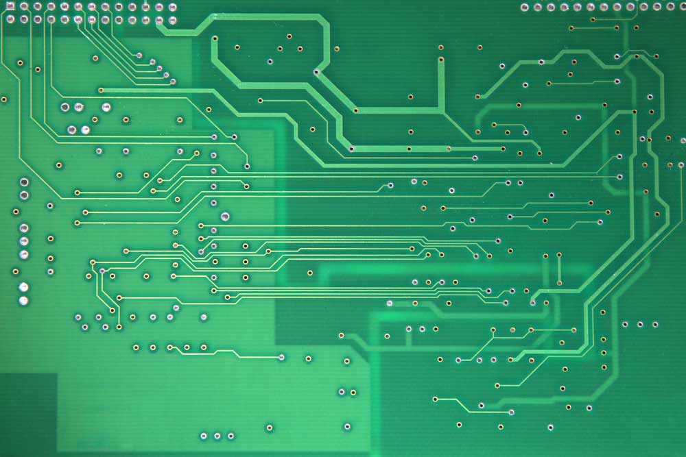
Layout file: describes the basic PCB layout.
Component Placement File: Describes the location of individual components.
Assembly drawings and instructions explains how to assemble the board.
User Guides: Although not required, they are useful for providing additional information to the user.
Gerber File Set: A set of layout output files that the PCB manufacturer will use to create the PCB.
PCB layout and design guidelines
In the process of wiring and designing printed circuit boards, many nuances must be taken into account. Some considerations apply to the entire process and some to individual steps. Here are seven important factors to keep in mind.
Fee restrictions in PCB
The first restrictions that you should pay attention to are related to the board that has not yet been completed. Some of these major limitations include the size and shape of the board itself.
You will need to make sure you have enough space on the board for the circuit right away. The size of the end product, the functionality the board needs to provide, and other factors determine how big it needs to be.
Before you start designing, estimate the approximate size of the board. If you don't have enough space for all the features required in a simpler design, you may need to use a fiberglass laminate or High-Density Interconnect (HDI) method.
The standard printed circuit board has a rectangular shape. In the vast majority of cases, it remains the most common form of printed circuit boards. However, boards of other shapes can also be created. Most often, developers do this because of size restrictions or to use irregularly shaped elements.
Number of Layers According to Power Level
Another important point is the number of required layers, which is determined by the power level and the complexity of the design. It's best to figure out how many layers you need early in your layout design.
Adding more layers may increase production costs, but will allow you to include more tracks. This may be required for more complex boards with advanced functionality.
For all high-current traces, use at least two holes for layer transitions. The use of multiple vias at the transition to other layers improves reliability, improves thermal conductivity, and reduces inductive and resistive losses.
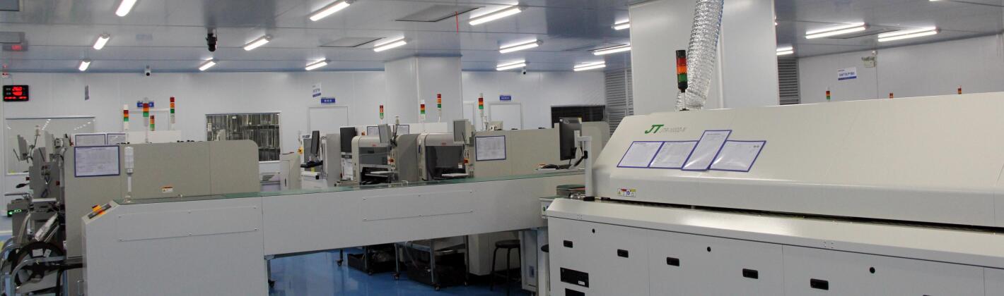
Manufacturing processes
You should also take into account the manufacturing processes that you would like to use to make the board. Different methods have different limitations and difficulties. You will need to use the reference holes or points that will be needed during the fabrication of the board.
Also, do not forget about the method of mounting the board. Different approaches may require different areas of the board to be left open. Using multiple types of technologies such as through holes and surface mount components can increase the cost of your boards, but may be necessary in some cases.
Always check with the manufacturer to see if they can make the type of board you need. Some of them, for example, may not be able to fulfill your order with a large number of layers or boards using a flexible design.
Materials and components
During the layout phase, consider what materials and components you plan to use for your board. First of all, you need to make sure that the required elements are available. Some materials and parts are hard to find, while others are so expensive that they can't be found.
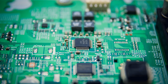
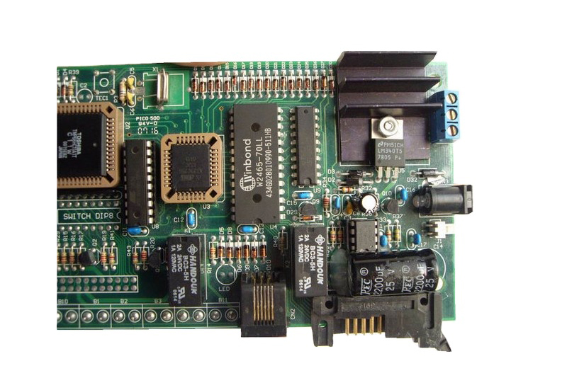
Component Placement Order
One of the most basic PCB design rules involves the order in which components are placed on the board. Recommended order: connectors, then power circuits, then precise circuits, then critical circuits, and then the rest of the elements. Power levels, noise susceptibility, generation, and routable capability also affect circuit routing priority.
Orientation
When placing components, try to orient them in the same direction, mostly those that are similar to each other. This will make the soldering process more efficient and help avoid mistakes during the process.
Accommodation
Avoid placing parts on the solder side of the PCB that will be behind the through-hole-covered areas.
Formation
The logical formation of components can reduce the number of necessary assembly steps, increase efficiency and reduce costs. Try to place all surface mount components on one side of the board and all through-hole components on the top side.
Comment on this article here
-
No comment

Ripple
Hi everyone, I'm Ripple, Sales Director of KFPCBA Tech Ltd. If you are looking for a one-stop PCB and PCB assembly manufacturer in China, KFPCBA is your best choice! Please feel free to contact our team! Thanks!
Contact me now


