


 tel:+86-18825224069
 email:
 address:201, Factory 6, Longhui Industrial Park, Fuqiao 3rd District, Xinhe Community, Fuhai Street, Baoan District, Shenzhen china
PCB stackup : multilayer circuit design of complex devices
Release date:2022-02-15 13:55:33 Number of views:0
Since the electronic device is more complex every day, it is more economical to assemble more complex circuits in compact space. The best solution replaces the build multiple panels, which are stacked in multiple layers. Therefore, multilayer circuit board stacking design is one of the key steps in the board design process, and we study in detail below. Take a look!
What is PCB Stackup?
A stack is a pile of objects, so a PCB stack has an accumulation of circuit layers. In technical terms, it refers to the insulating and copper layer arrangement that make up the circuit board.
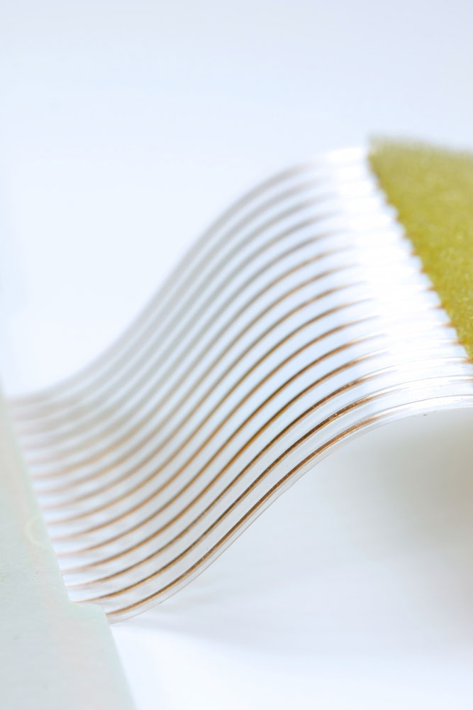
A multilayer PCB
Source: Wikimedia Commons More specifically, it refers to the number of layers, the space between them, and the materials used in the fabrication process. You need to complete the PCB layer stack up before rounding up the board layout design, and this involves arranging the layers, prepregs, laminations, cores, vias, etc. The proper stack-up renders noise-free signals, circuit integrity,
and a high-quality PCB if done correctly. PCB layers
Why Need Stackup?
Whether using a 4layer, 6layer, 8layer, or more, the layer stack-up effectively reduces crosstalk and electromagnetic radiation while enhancing signal integrity. As a result, it creates a low-inductance power network while also improving product manufacturability. However, you can only get these benefits if you design the multilayer correctly as per the EMC requirements, circuit size, and PCB size. Also, you should determine the number & location of the inner layers and how to distribute signals in these layers. Otherwise, you will end up with a poorly designed PCB, which will reduce the signal transmission's electrical performance. Consequently, you will get a circuit with more noise, emissions, and crosstalk.
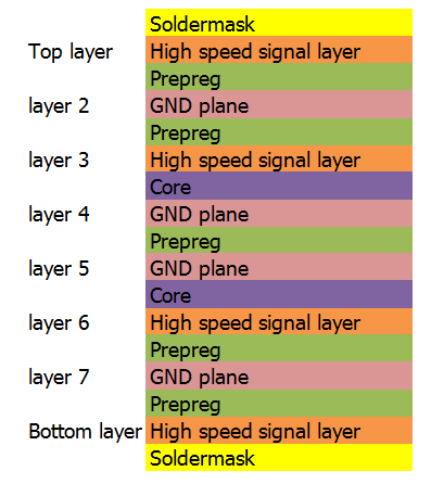
The PCB Stack-up Structure
Typically, board stack-ups consist of alternating layers of copper foil, core, and prepreg materials, all glued and heat-pressed together. Usually, the core material is a weaved fiberglass material cured with epoxy resin. It forms a thin dielectric that insulates the thin adjacent copper layers. Also, the prepreg binds all the internal layers. When deciding on the number of layers, consider these factors:
Component density and package types
Board complexity
Ground/power/signal layer requirements
Additionally, accommodate channel routing with blind vias to get the best signal integrity for high-channel density devices.
An example of an 8-layer pcb stack up
The Benefits of PCB Stackup
Maximizes the function of the circuit board
Improves durability
Effectively minimizes radiation, signal crosstalk, and impedance on high-speed, high-frequency circuit boards.
Reduces manufacturing costs
Connects multiple circuits
Enhances the PCB's efficiency
Provides unique connection points for all electronic components
Compact and lightweight design
Enhances electromagnetic compatibility
Standard 4 Layer PCB Stackup
The standard 4-layer stack up features four evenly-spaced films with planes in the middle. Even though such boards are perfectly symmetrical, this does not assist the electromagnetic compatibility (EMC). Similarly, coupling the layers closely in the center with large dielectric layers between the planes and signal layers does not help with crosstalk, EMC, or signal integrity. That said, it develops favorable interplane capacitance, but the cons outweigh the pros, which is why a 4-layer PCB is better than the dual-layer type.
An example of a 4-layer PCB stack up In a 4-layer board, we improve the EMC performance by positioning the signal layers near the planes, usually <10mil. Also, we use a large core (about 40mil) between the ground and power plane to keep the substrate's standard thickness to about 2mil.
Standard 6 Layer PCB Stackup
If you add two signal layers to a 4-layer board, you get a 6-layer PCB. The extra layers dramatically enhance electromagnetic interference because the board features two inner high-speed and two outer low-speed signal planes.
An example of a 6-layer PCB stack up
The signal planes should be close to the adjacent planes to keep the board thickness within 62mil. When building this stack up, you have to balance the core thickness, trace width, & impedance.
Standard 8 Layer PCB Stackup
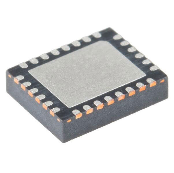
The 8-layer stack up improves EMC performance by adding two signal planes to the 6-layer PCB stack up. Adding these to the substrate center allows tight coupling between the middle planes. Also, it separates each signal layer to reduce coupling, which minimizes crosstalk dramatically. DDR2 and DDR3 memory usually use this configuration because the tight routing does not cause a crosstalk issue.
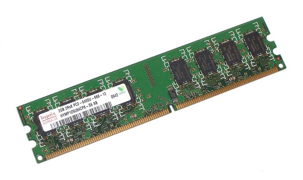
2GB DDR2 memory
Source: Wikimedia Commons However, it is vital to note that having more than two adjacent signal layers between the planes leads to impedance discontinuities. It can be up to a 20-ohm impedance difference, which increases crosstalk.
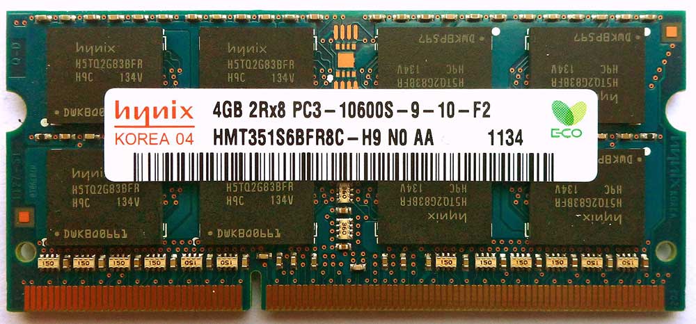
4GB DDR3 memorySource: Wikimedia Commons
Top Tips for PCB Stackup Design
Determining The Number of Layers
Of course, the first consideration is the number of layers. To clarify, you need to consider the following:
Power (for high power boards or when your circuit features power supplies)
Ground planes/layers
Signal (low or high speed)
Ideally, the best design should not mix the signal types in the core layers. To get the accurate layer count, you can first calculate the pin density using this formula: Pin density = Board area / (Total number of pins/14) After getting the pin density, use this lookup table to find the signal layer count.
| Pin Density | Number of Signal Layers | Number of Board Layers |
| >1.0 | 2 | 2 |
| 0.6 - 1.0 | 2 | 4 |
| 0.4 - 0.6 | 4 | 6 |
| 0.3 - 0.4 | 6 | 8 |
| 0.2 - 0.3 | 8 | 12 |
| <0.2 | 10 | 14 |
Determining The Layer Arrangement
Secondly, determine the number of layers and their arrangement. Use these rules:
Avoid placing two signal layers next to each other
Keep the stack up symmetric going inward from the top & bottom layers
Route the high-speed signals on minimum thickness microstrips
Maintain minimal spacing between the power and ground layers
Keep the internal power layers next to the signal layers for tight coupling
Determining Layer Material Types
Next, determine the thickness of each signal layer plus the core and prepreg. Although there are standard PCB material type thicknesses, you should consider each material's thermal, electrical, and mechanical properties.
Determining Routing and Vias
Lastly, determine the routing traces by deciding on:
The copper weights
Where to place the vias
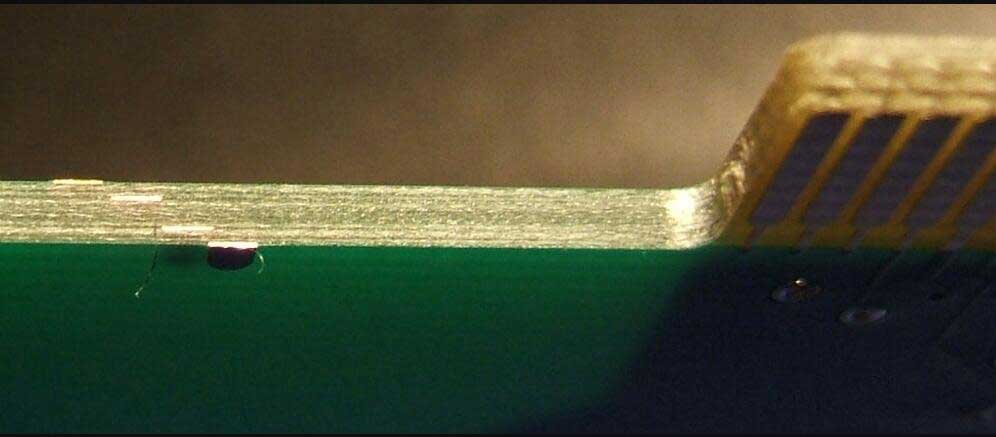
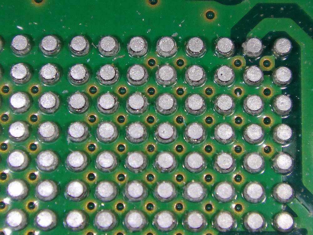
PCB vias
The Difference Between Standard Stack-Up and HDI Stack-UpHDI is an acronym for High-Density Interconnect, so the stack-up has the following advantages over the standard stack-up.
Low aspect ratio
Few layers
High component density per square inch
The cutting-edge technology revolutionizes multilayer circuit board design and fabrication by offering a sequential build-up for stack-up. Therefore, you get a wide variety of designs while simplifying the architecture for complex boards. Additionally, the stack uses stacked, buried, blind, staggered vias. The highest pin count device and quantity of ball grid arrays determine the layer count. Also, the number of power, signal, and ground layers affect the HDI, but the recommended plane and signal layer numbers should be even. The goal is to create a balanced, symmetric structure.
On the other hand, the standard stack-up design depends on several factors, such as the:
Number of signal layers, ground planes, and power planes
Emission requirements
Layers sequence
Circuit frequency
Distance between layers
Shielded/unshielded enclosure
Therefore, the essential design rules for the standard stack up include spacing the signal layers and having wide cores to prevent EMC issues. One of the key benefits of this layering is the inner layer shielding. But the disadvantage is ground plane reduction due to component mounting pads, especially on high-density PCBs.
Summary
In conclusion, PCB stack-up is essential in modern, complex devices because it places large circuits in a small space. At KFPCBA, we have the expertise and experience to deliver the highest quality PCB that meets all standards. If you need a circuit board for your project, contact us for more details. You can also submit your design for fabrication.
Comment on this article here
-
No comment

Ripple
Hi everyone, I'm Ripple, Sales Director of KFPCBA Tech Ltd. If you are looking for a one-stop PCB and PCB assembly manufacturer in China, KFPCBA is your best choice! Please feel free to contact our team! Thanks!
Contact me now


