


 tel:+86-18825224069
 email:
 address:201, Factory 6, Longhui Industrial Park, Fuqiao 3rd District, Xinhe Community, Fuhai Street, Baoan District, Shenzhen china
How PCB Assembly Defect Detection System Ensures Product Quality
Release date:2022-04-22 14:51:40 Number of views:0
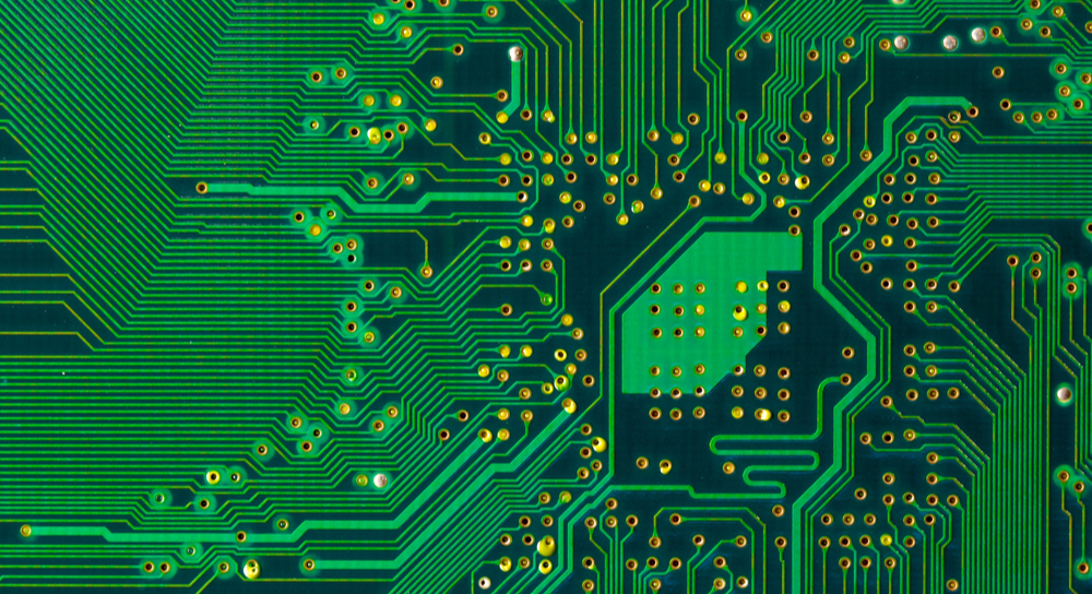
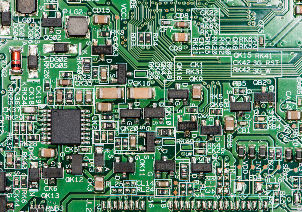
The PCB assembly process requires collective and constant attention to ensure the quality of the final product. In the absence of a reliable PCB assembly defect detection system, misaligned components or bad pads can be missed despite careful manual testing. If you're lucky, it might cost you some extra work. Worst case scenario: You just lost your entire project. Let's take a look at some common PCB defects, understand their impact on the quality of the final product, and see how to avoid them completely with the right trouble-free testing strategies.
Common PCB Defects and Their Impact on Product Quality
brazed bridge
Defined as a defect according to IPC-A-610D, a solder bridge is formed when two component pads on a printed circuit board that are not intended to be electrically bonded are bonded together due to the use of excess solder. Even a small jumper can create a conductive path between components and cause a component to short or burn out. Early detection of print defects immediately after the print operation and before component placement saves PCB manufacturers time and costly rework when assembling defective boards.

tombstone
Also known as the Manhattan effect or the alligator effect, the tombstone effect refers to the partial or full uplift of the soldering process of passive SMT components during PCB reflow. This may be due to different wetting rates, poor gasket design, PCB contamination, or incorrect gasket size. The tombstone phenomenon directly affects the quality and reliability of the PCB, and will lead to additional maintenance costs if not detected in time.
job change
Sometimes when surface mounting a mounting device (P&P), wet solder paste components can move around. This slight position shift is usually underestimated and is considered to be noticeable during reflow soldering. Component displacement can occur due to poor quality solder paste, excessive flux consumption during reflow, improper handling of the component after the P&P process, or insufficient air pressure at the nozzle. Once a component is moved, it affects the overall performance and reliability of the board.
Ribbon
PCBs sometimes contain webs of solder and flux residue. These solder residues are called solder strips. Jumpers can occur for many reasons, including solder contamination, extensive mask contamination, or resin curing errors on the board. This can adversely affect the quality of the solder joints, leading to unreliable signal transmission and "burials".
stomata
Porosity, or pinholes, is associated with moisture escaping from through-hole boards through thin copper plating or voids during wave soldering. Excessive moisture, poor flux or drilling through bare board, and gaps between coating and laminate can cause porosity. Initially, these holes may be limited to certain places, but gradually spread throughout the board.
Problems with Traditional Troubleshooting Strategies
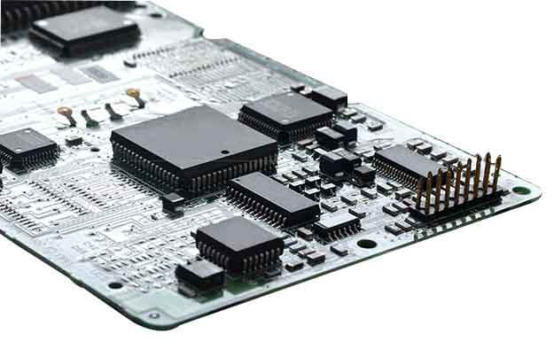
Without a proper automated PCB assembly defect detection system, a lot of manual work is required. More traditional PCB troubleshooting strategies often involve many tedious steps. First, you should perform a visual inspection to track down simple problems such as solder bridges, tombstones, and package mismatches. If the board passed the first stage, it's time to check it for possible build defects or faulty components. If all else fails, removing the component from the board and testing it for the desired functionality should be your last step; however, if the component is very small or has thick pins, you may find it difficult to recreate it with solder on the board.

This process can be tedious and time consuming, increasing the chances of human error, design flaws, rework, and lead time (despite following a comprehensive troubleshooting strategy).
The Engineer's Guide to PCB Manufacturing Complexity
Download now
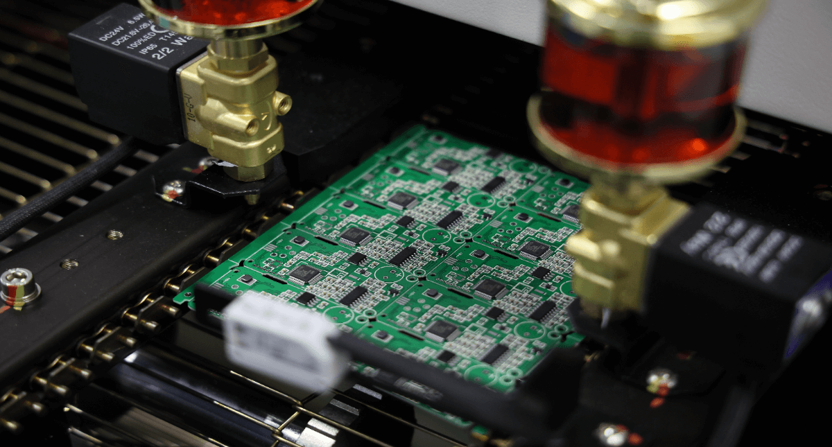
Improving Product Quality with Automated PCB Assembly Defect Detection Systems
When your PCB assembly defect detection system includes highly reliable, versatile automated robots, you have little room for error.
Solder Paste Control (SPI)
3D solder paste inspection machines are an important element in the PCB assembly process. It checks solder paste deposits, including their shape, volume and coverage, and provides instant feedback via a graphical interface. Early detection systems help manufacturers avoid.
Comment on this article here
-
No comment

Ripple
Hi everyone, I'm Ripple, Sales Director of KFPCBA Tech Ltd. If you are looking for a one-stop PCB and PCB assembly manufacturer in China, KFPCBA is your best choice! Please feel free to contact our team! Thanks!
Contact me now
Relevant content you may be interested in
Related articles


