


 tel:+86-18825224069
 email:
 address:201, Factory 6, Longhui Industrial Park, Fuqiao 3rd District, Xinhe Community, Fuhai Street, Baoan District, Shenzhen china
Can increasing solder paste improve poor BGA welding?
Release date:2022-04-27 17:40:24 Number of views:0
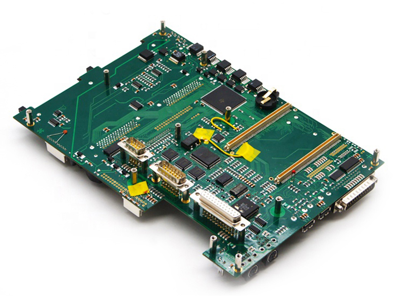
How to improve BGA welding quality is one of the continuous quality improvement goals of SMT engineers, especially for BGA parts with fine pitch. Generally, we call BGA pitch below 0.8mm as fine pitch (sometimes different definitions will be a little different).
The reason why BGA is difficult to weld is that its solder joints are all concentrated below its body, and it is difficult to check its welding quality by visual inspection or AOI (Auto Optical Inspector) image detection instrument after welding. Sometimes, it is difficult to judge whether it is empty welding or false welding even using X-ray. (Some rotatable X-ray or 5DX machines have the opportunity to inspect BGA for air welding problems, but these X-ray inspection machines are expensive and do not seem to reach the economic scale of on-line inspection.

Experience tells us that the most important quality problems after BGA welding are almost concentrated In HIP (head-in-pillow effect, double ball effect). This is because when the circuit board (PCB) passes through the high temperature zone of Reflow, it is easy to cause the deformation of PCB plate and BGA body. When the solder paste and BGA tin ball melt into liquid state, they are separated from each other and do not touch each other. When the circuit board temperature drops and is lower than the melting point of solder, the deformation of PCB and BGA body gradually decreases. However, the solder paste and the solder ball have condensed back into a solid state, resulting in the formation of a double ball overlapping solder phenomenon, known as HIP.
More than 90% HIP occurs in the outermost tin ball or its four corners of BGA, because the distance of the diagonal of BGA packaging is the longest, and the relative deformation is the most serious. The second serious deformation is in the outermost tin ball of BGA.

Based on the above experience, as well as the experiments conducted by many SMT predecessors, increasing the solder content of BGA can effectively reduce the HIP problems caused by temperature deformation. But be careful if the amount of solder paste increases too much, it will cause the problem of welding short circuit, not careless.
Therefore, the method chosen by the following working bear is to increase the solder paste content of BGA locally rather than increase the solder content of all solder ball pads.
Change the BGA solder paste volume can come from the steel plate (font), the basic principle is to make the BGA outside a row or the four corners of the tin solder paste printing, than the rest of the other more amount of solder paste, solder ball but not too much more, such ability can still maintain enough when PCB and BGA ontology deformation of solder paste and BGA solder ball in contact with the underneath.
The method chosen by the working bear is to increase the solder paste of BGA locally rather than increase the solder paste of the whole solder ball pad.
When BGA tin ball is greater than 0.4mm:
Increase the amount of solder paste printing on the four sides of the outer BGA, open the steel plate into a square and form an inner circle with the original solder ball welding pad, and maintain the original amount of other solder ball welding pads.
When BGA tin ball is less than 0.4mm:
The solder paste printing on the outer four sides of THE BGA will remain unchanged, but the solder paste printing on the other inner balls will be reduced, and the steel plate will be square to form an outer circle with the original solder pad.
In this way, regardless of the size of BGA, the solder paste of the outermost ring is about 16.7% more than that of the inner ring, to ensure that there is enough solder paste to keep contact with the solder ball under BGA when the PCB and BGA body flow through high temperature deformation.
The following picture shows that the size of BGA tin ball is less than 0.4mm. X-ray was obtained by reducing the amount of tin paste in the inner ring of BGA ball. After a little attention, it can be found that the amount of tin in the outermost ring (the diameter of the circle) is a little more than that in other inner rings. So the black circle on the outside is a little bit larger in diameter than the black circle on the inside.
Comment on this article here
-
No comment

Ripple
Hi everyone, I'm Ripple, Sales Director of KFPCBA Tech Ltd. If you are looking for a one-stop PCB and PCB assembly manufacturer in China, KFPCBA is your best choice! Please feel free to contact our team! Thanks!
Contact me now
Relevant content you may be interested in
Related articles


