


 tel:+86-18825224069
 email:
 address:201, Factory 6, Longhui Industrial Park, Fuqiao 3rd District, Xinhe Community, Fuhai Street, Baoan District, Shenzhen china
PCB design Clearance and Creepage calculator: Rules and Calculation
Release date:2022-09-20 14:37:08 Number of views:0
In PCB design, equipment safety requirements such as clearance and creepage distances are crucial. These factors help in the smooth operating conditions, possible failure, and other environmental conditions affecting electronics. These conditions are pollution, altitude, humidity, and temperature. As a result, these PCB safety standards come with regulations and clear statements. So, eventually, end-users get the best out of their high-quality products.

Further, you learn all about these safety standards. The primary aim is to limit the hazards of electric shock to humans. In addition, you learn the best insulation methods, ideal insulation materials, and clearance and creepage distance for electronic products.
What are clearance and creepage distances?
Why do we calculate Clearance and Creepage distance?
Classes of equipment to protect from electric shock
Important factors in determining distance
4.1. Insulation type
The example of distance calculation
Measurement of creepage distances and clearances
Design guidelines for PCB creepage and clearance issue
What Are the PCB Creepage and Clearance Standards?
Conclusion
What are clearance and creepage distances?
What is clearance?
Electrical clearance refers to the shortest distance of air between two conductive materials. It provides adequate isolation against impulse voltage. It is otherwise called transient overvoltages.
Creepage and clearance requirements are related to isolator working voltage due to the possibility of arcing resulting from charge buildup and transfer. This scenario occurs on the device's surface after an extended operation period under high working voltages. Examples of large clearances in voltage circuits involve vibration and applied forces.

(A result of transient overvoltages).
What is creepage?
Meanwhile, PCB creepage distance is the shortest distance along a solid insulating material's conductive ends. Work out the existing long-term AC voltage in the voltage board to determine PCB creepage distance. To some, it is the basic operating voltage in voltage circuits. To others, it is the rated insulation voltage.
Typically, the requirements for creepage surface distance indicate that it is not below the corresponding clearance. The required clearance is equal to the minimum creepage distance. Also, there is a direct relationship between the minimum creepage distance and the minimum clearance distance in the air.
Why do we calculate Clearance and Creepage distance?
Apart from isolation for operator safety, it is an important design rule to calculate creepage surface distance and clearance.
It helps improve product design and the overall safety of mechatronic elements. Hence, industries such as automotive, aerospace, defense, and high-tech electronics receive protection from shock risks.
Also, it ensures protection from arcing failure and overall circuit damage caused by hazardous voltage.
You optimize the design process with additional electromechanical safety methods like Creo Clearance and Creepage extension.
Again, it helps automate a direct digital model analysis and receive visual feedback.
It reduces production error and reworks.
Further, it saves time and prototype costs.
It also helps reduce product recalls and damage to warranty claims.
Apart from isolation for operator safety, it is an important design rule to calculate creepage surface distance and clearance.
Classes of equipment to protect from electric shock
Class I equipment
Alongside the basic protection, it gives a vertical barrier for added protective cover. This voltage insulator conducts hazardous breakdown voltage down to the earth. In that case, the external wires link to the conductor's protective earthing when board insulation breaks down.
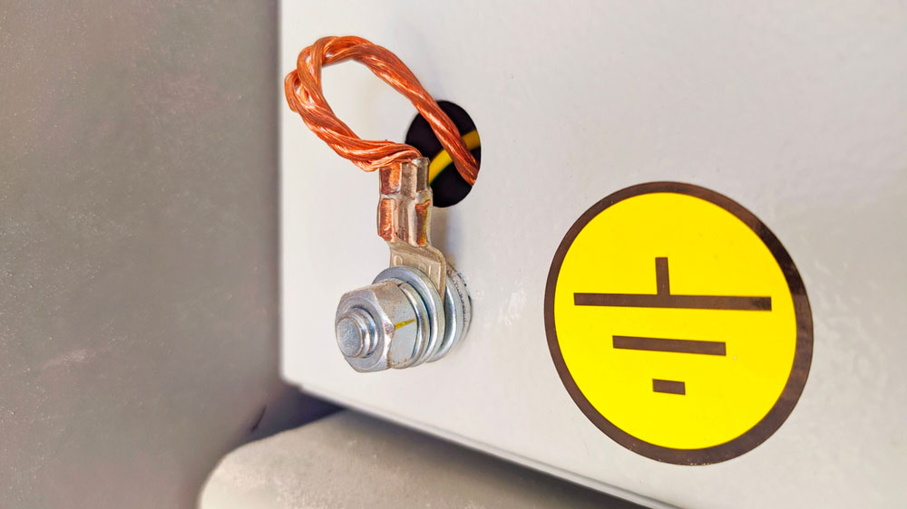
(An insulating electrical earthing circuit showing ground sign)
Class II equipment
Acts as a sheet barrier for electric shock protection like Class I equipment. However, it lacks ground protection. Instead, it provides reinforced insulation against electric shock.
Class III equipment
In this aspect, there are no dangerous voltages as the PCB material has insulation barriers. Therefore, the energy neither causes injury nor pain.
Important factors in determining distance
The major factors that influence creepage and clearance distance are
Insulation.
Input voltage.
Material group.
Overvoltage category.
Pollution degree.
Altitude.
4.1. Insulation type
Further, the insulation types depend on their different purposes. The standards are
Basic insulation.
It provides single-layer insulation for users against electric shocks and electrical breakdowns.
Double insulation
Provides basic and supplementary insulation benefits.
Functional insulation
It only provides insulation at the conductive points of the equipment.
Reinforced insulation
It is a single-layer insulation type that provides double insulation protection properties.
Supplementary insulation
In addition to second-layer protection, it protects the user from basic insulation failure.
As for insulation materials in electronic circuits, the major ones are
FR-2:
This IC substrate is low-rated insulation against flaming; hence, its name is flame resistant 2. It is built from phenolic material and paper. It is portable and generally reliable for many purposes. Also, it is halogen-free insulation material. However, it is popular among consumer electronics because it is cheap.
FR-4:
The FR4 is a higher grade of flame-resistant laminate. It is relatively more popular than FR2 and yet affordable. It is most often used in twofold PCB and multilayer circuit boards. FR4 is also great at withstanding high temperatures in high-voltage design applications.
RF:
This substrate insulation material is a mainstay in microwave ovens, military electronic devices, medical devices, etc. RF circuits utilize low dielectric plastic as an insulation barrier.
Flex:
As its name implies, the insulation material is for flexible applications such as flex circuits. These circuits rely on tiny flexible plastics for insulation.
Metal:
It is awkward to mention the term "metal insulators." However, in this case, it acts as a detector. As such, the metal melts when there are unexpected conductive charges on your PCB. Therefore, causing an open circuit situation and insulating the circuit in the process.
4.2. Material Group
To distinguish the different material groups, you need a Comparative Tracking Index. They are
Material Group 1: 600 ≤ CTI
Material Group 2:400 ≤ CTI < 600.
Material Group 3a:175 ≤ CTI < 400.
Material Group 3b:100 ≤ CTI < 175.
Material group 3b, generally, is a group of unknown materials.
4.3.Pollution degree
According to IEC 62368, there are various degrees of pollution.
Pollution degree 1
This pollution degree is dry and non-conductive. These include moisture and dust that enter through the sealed packages of subassemblies, components, and equipment.
Pollution degree 2
Here, non-conductive pollution happens unless there is condensation. Often, it is common in general laboratories and office environments.
Pollution degree 3
This type involves conductive pollution. Otherwise, an expected condensation induces non-conductive pollution. It happens among factory equipment.
4.4. Overvoltage category
Knowing the device overvoltage category is important before connecting to the power supply. In addition, determine the device's transient voltage in connection to its input terminals.
Overvoltage category 1:
The first category helps limit power transients.
Overvoltage category 2:
This category enables safe pluggable equipment via the building wiring.
Overvoltage category 3:
The equipment and building wiring are crucial to knowing the overvoltage category here.
Overvoltage category 4:
Here, the main power supply in the building connects the conductive paths to equipment directly.
4.5. Altitude
The ideal altitude requirement for equipment clearance is below 2KM above sea level. Otherwise, you must multiply the different altitude correction factors by the obtained clearances.
See the IEC 62368-1 table for the PCB creepage and clearance base factors.
The example of distance calculation
The basic insulation distance differs between the power converters' primary and secondary sides. A good example is the AC/DC converter with an input voltage of 100-240Vac. The table below helps calculate the shortest path for creepage and clearance distance for insulation.
| AC mains voltage (a) | Mains transient voltage (b) | ||||
| Overvoltage category(V peak) | |||||
| Vr.m.s. | V peak(c) | I | II | III | IV |
| 50 | 71 | 330 | 500 | 800 | 1500 |
| 100d | 141 | 500 | 800 | 1500 | 2500 |
| 150e | 210 | 800 | 1500 | 2500 | 4000 |
| 300f | 420 | 1500 | 2500 | 4000 | 6000 |
| 600g | 840 | 2500 | 4000 | 6000 | 8000 |
Measurement of creepage distances and clearances
There are many examples of creepage and clearance distance measurements. Normally, you compare the value of X to the pollution degree. But ignore the groove or gap width if it goes below X mm. However, if it equals or exceeds Xmm, measure the creepage distance along the groove contour.
(PCB with a V-groove contour).
Table of IEC 62368-1 standard
| Pollution degree | X (mm) |
| 1 | 0.25 |
| 2 | 1.00 |
| 3 | 1.50 |
Design guidelines for PCB creepage and clearance issue
The commonest solution for PCB clearance and creepage issues is to expand the distance between conductors or components. However, it is fast becoming irrelevant due to the popularity of high-density PCBs and the shrinking form factor. However, more specific guidelines include
Clearance- Add a barrier between the nodes or conductors to insulate the air distance. On a double-sided panel, you place high-voltage and low-voltage components on the top and bottom, respectively. Overall, insulating the PCB substrate is a great idea.
Creepage- A valid method of dealing with creepage issues is to create a valley between the node peaks. Also, it is useful to cut a trough or groove in the PCB substrate. Like power line insulators, another useful method is to cut ridges or slots along the entire insulator length.
Material- The insulation material selection also matters in creepage issues. Voltages often create conductive paths along an insulator's surface. Therefore, a lower CTI in a material is more susceptible to this creepage fault and vice versa.
Bounding Surface - Like its conductors, clearance and creepage are properties of a PCB's enclosure. Therefore, it is important to consider this factor when designing a PCB with your mechanical engineer.
What Are the PCB Creepage and Clearance Standards?
There are a couple of helpful clearance standards and creepage requirements. However, the IPC 2221 and IEC 60601 certifications are the two major ones. These creepage and clearance requirements help to identify the conductor spacings for different scenarios and voltages.
In most cases, the best testing service for clearance and creepage requirements is Underwriter's Laboratory (UL). An example is the UL61010-1: Electrical Equipment.
Conclusion
In summary, electronic products need a set creepage and clearance distance for crucial protection from shock and damage. Many factors, such as the environment, product location, and material type, help influence the design of these electronics.
Therefore, no matter your project, you need a quality manufacturer for the highest quality PCB design standards. And if you need to get rid of familiar clearance and creepage distance issues, contact us.
Comment on this article here
-
No comment

Ripple
Hi everyone, I'm Ripple, Sales Director of KFPCBA Tech Ltd. If you are looking for a one-stop PCB and PCB assembly manufacturer in China, KFPCBA is your best choice! Please feel free to contact our team! Thanks!
Contact me now
Relevant content you may be interested in
Related articles


