


 tel:+86-18825224069
 email:
 address:201, Factory 6, Longhui Industrial Park, Fuqiao 3rd District, Xinhe Community, Fuhai Street, Baoan District, Shenzhen china
Important Things You Need to Know About How to Design PCB
Release date:2022-08-12 11:01:59 Number of views:0
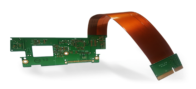
Preparing a PCB prototype on a breadboard and finally starting to design your PCB are two different things. Before you begin planning a PCB, there is not much you need to know first. So, it is time to dive into how to design PCB. It is not going to be an easy task. You will have to go through challenging steps from step one to step two.
Basics of PCB designing you need to know about
How your device will work depends on the design of the PCB. You are going to need different electronics to create a PCB. There are a few basic things about the PCB that you need to know before you start working on the actual task:
Size of PCB
Primarily the size of the PCB gets decided according to the device's size. Make sure you are choosing the right size of PCB that will fit inside the product you are designing the circuit for.
Layers on PCB
There is a fact about the layers on the PCB that the more layers mean, the more complex design you will work on. Plus, the layers are going to be expensive.
Two layers
A PCB with two layers is for toy products.
Four layers
A PCB with four layers is for IoT-linked products.
Six layers
A PCB with six layers is for smartwatch and smartphones.
PCB requirements
If you are going to design the PCB for someone else or your use, there are a few things that you need to know. You must know about all the PCB-creating basic requirements like trace sizes, pacing, power isolation, and film naming.
Information you need to save before you start designing the PCB
Material
Number of layers
Thickness of PCB
Color
Surface finish
Weight of copper
Gerber file
How to design a PCB step-by-step guide?
If you have been looking for answers to a question about how to design PCB, then here are all the steps that are going to be required to design PCB:
PCB circuit design
The first step of designing a PCB is to develop a schematic. Yes, a document or a blueprint explaining how the components on the PCB will relate to each other and how they will work together. You are going to need software to create the schematic document. Quadcept is a reliable software for the job as it has been designed for PCB design.
Now you have to get component information of all the components you will install on the PCB. You get this information from your vendor.
Once you make a list, you must enter those details into the software. The data gets uploaded on the software; after that, you must pin all the components together.
A schematic file is going to be the footprint of the PCB you are going to design.
It must have information about the physical dimensions of the PCB components and the copper pad placements or through holes on the board.
You need to select the components in advance and ensure they are available in the market.
The schematic document is going to be your reference file. You can tell the details from that file if you forget something. It will save from making any mistakes while designing the PCB. So, the first step of how to design PCB is to get started with the schematic file.

Layout & Gerber file
Once you complete the schematic file, you can use the same software to create a Gerber file. This file will be the layout of the component allocation on the PCB. Plus, how all the components will get connected through the PCB layers. You need to keep in mind that the more layers you are going to design, the more complex the PCB becomes.
First, you must divide the PCB into logical parts according to its functionality. Once you separate the board into logical parts, you need to group the components in the related areas. If you do this, you can reduce noise, keep conductive traces short, and interfere.
Now the second step is that you need to keep UI in your mind while you are designing your PCB. For perfect user experience, you need to adjust the components like connectors, LEDs, audio jacks etc., in the most convenient locations.
Once you are done with the designing layout of the PCB now, it becomes the Gerber file.
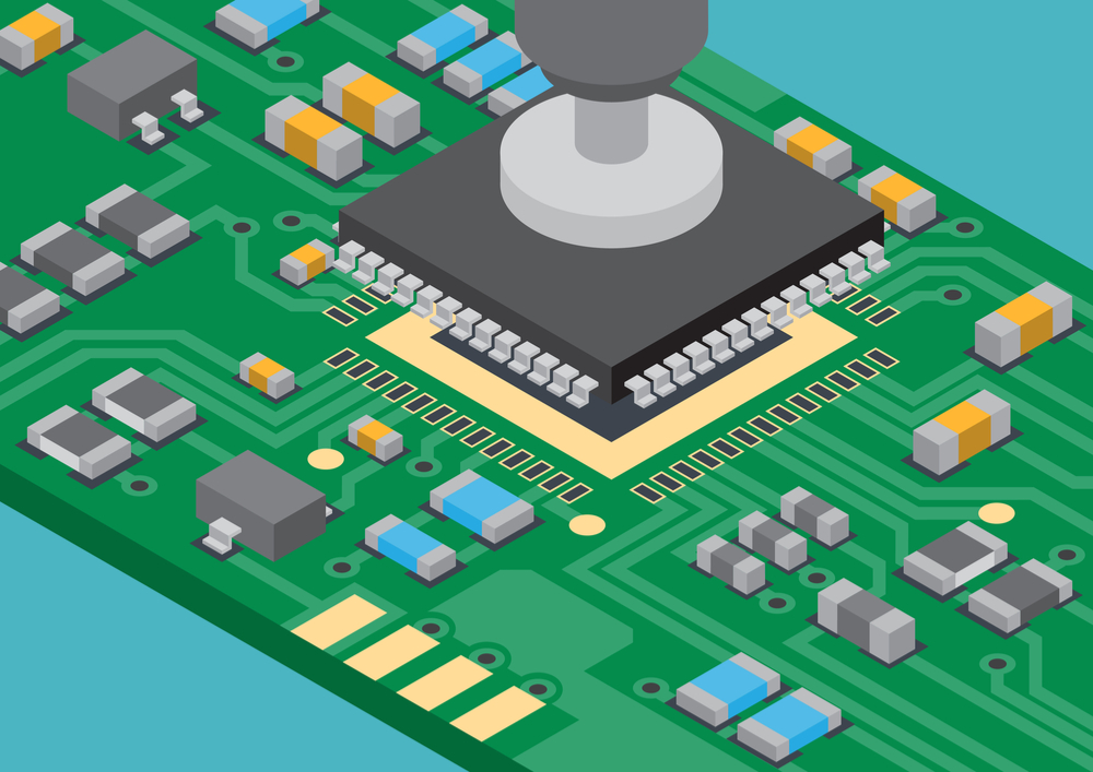
It is going to help in designing the PCB in reality. Placement of all the components on the PCB in the right way is very much important. There might be a situation where the elements interfere with one another if not placed correctly. So, you must ensure that you put them in the correct location. Otherwise, if you end up causing any mistake you might have to start the whole designing process from scratch.
PCB fabrication process
Once your Gerber file is ready, it is time to do the actual work. It is time to get the board printed on a circuit board. It is essential to start a different process, like adding components to the board.
Prepare material
To this step, you would be done with component selection, and now you have to order them. There are a few essential tips that you need to keep in mind before the actual work starts:
Components delivery time
You might not get all the components from a single vendor. The delivery time of receiving the parts can be up to 8-16 weeks. So, make the order at the right time.
Packaging of components
Instead of separate packaging, you should order components in reels.
Minimum quantity of order
You need to order components in stock.
Time for mounting components PCB
There are two techniques for mounting components on PCB. Let's discuss both methods in detail:
Surface Mount Technology
Commonly surface mount technology is used for manufacturing PCB on a large scale. Accurate and fast SMT machines are used to complete the task to save time, human error and money.
Through-hole
It is a manual way of fitting all the components on the PCB. It consumes so much time and might delay your project too.
Soldering
To ensure that all the components stick to the PCB ideally, you might have to do soldering. Yes, it will make the components attached to the PCB, and they won't come out after that.
The PCB goes through an infrared lamp, and the light heat heats the board until the solder melts. Once the solder melts, it connects the components permanently to the PCB.
Every single component will have its thermal heat-bearing capacity, so you need to ensure that the soldering process doesn't cause any damage to them.
Other Soldering techniques
There are two other soldering techniques that you must know:
Iron soldering
These soldering techniques work in rare cases. If you are going to manufacture PCB in bulk, then this is the ideal solution for soldering.
Wave soldering
This soldering technique gets used on components that get added to the PCB through the thru-hole method. First, the PCB goes through the reflow soldering, and then after adding other parts, it manually goes through ware soldering.
Final testing step
It is necessary to get the PCB tested to ensure its quality. Without testing, never approve a PCB. There are a few mistakes that are pretty common to find in the PCB. Mistakes like misaligned components, components that are not connected properly, and shorts that connect different portions of the PCB should need to get connected, etc. So, here are a few standard tests for your PCB:
AOI
An automatic optical inspection. In this test, you need to have a golden sample to which you will compare your PCB. For this test, it is important and necessary the hardware creators provide you with the tolerance and specifications of the components. Your PCBA must pass this test and prove that it is equally perfect to the golden sample.
IT
An in-circuit test. While designing a PCB, you might leave some test points on the board for programming, debugging and many other reasons. The ICT machine will utilize those points in this test to do the short/open test. It will check whether the passive component values are within specifications or not.
X-Ray
The last test, one of the most important ones, is to check the soldering condition. What if the components don't stick to the board and fall off later? Anything can happen to the board if the soldering process has not been done accurately. So, with the help of an X-ray, the soldering condition gets checked for the ball grid array in this test.
Final Words:
Now you might have got the answer to your question about how to design PCB. We have discussed the steps of creating a PCB in the above details. You can get your PCB designed by someone else by providing them with all your requirements. Otherwise, if you are an electronic engineer yourself, then go ahead, follow the instructions and start designing your very own PCB.
Comment on this article here
-
No comment

Ripple
Hi everyone, I'm Ripple, Sales Director of KFPCBA Tech Ltd. If you are looking for a one-stop PCB and PCB assembly manufacturer in China, KFPCBA is your best choice! Please feel free to contact our team! Thanks!
Contact me now


