


 tel:+86-18825224069
 email:
 address:201, Factory 6, Longhui Industrial Park, Fuqiao 3rd District, Xinhe Community, Fuhai Street, Baoan District, Shenzhen china
PCB Design, Circuit Board Patch Don't Know How To Choose? (picture)
Release date:2022-11-23 16:12:03 Number of views:108
PCB design , circuit board patch don't know how to choose? (picture)
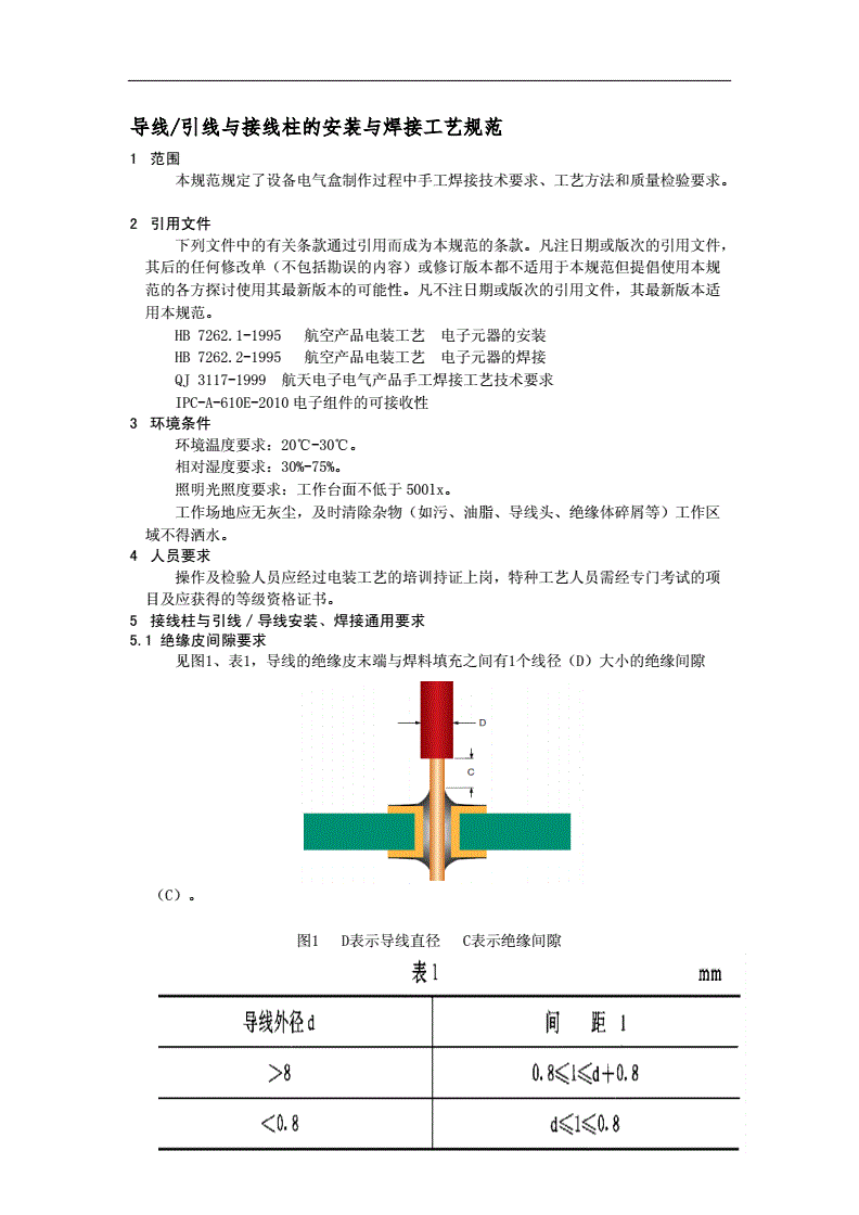
The unit of PCB basic PCB measurement PCB design originated in the United States, so its common unit is the nominal diameter of the thread, not the size of the metric plate. The size of the material is generally used in inches and the width of the electrical conductor is generally used in inches and feet. 1mil=1mil=.electrical conductor The thickness is often used in Gusi (oz) The typical weight of a square meter of metal material –=μm–=μm–=μm–=μm The cross-section of a typical 8-layer board A PCB is composed of continuously overlapping and Core materials : Core: A thin, dry and solid substance (usually FR4: glass fiber & epoxy resin based epoxy resin): Abbreviation. A thin piece of uncured material (generally FR4: glass fiber-epoxy resin) when heated or extruded, will melt in the epoxy resin glue, and then become and Core has the same relative dielectric constant of the raw material copper foil: a piece of copper coin, glued on both sides of the core with an epoxy resin. Copper layering is based on the symmetry of the positioning points of the board on the ordinate to prevent ground stress of mechanical equipment in the thermal cycle. PCB electrical conductors: Copper is a common electrical conductor in PCB. Routing should be done by electroplating gold for RF connectors. Provide a corrosion-resistant electrical transmission characteristic Width and length of wiring - controlled by PCB wiring engineers under normal manufacturing process. PCB design, circuit board patch don't know how to choose? Come here to buy easily! Beijing 8-layer pcb circuit board
The electromagnetic compatibility project method has a detection and modification method. During the design process, the electromagnetic compatibility design standard is adopted as much as possible. After the sample is completed, it is tested. OK, this approach is fine for very simple devices. But the project cost is relatively high; the control system design method carefully predicts and analyzes various possible EMC problems during the product design process, and adopts various countermeasures to prevent EMC problems from the very beginning of the design plan , This method can generally solve 80% of the electromagnetic compatibility problems before launching the product. EMC—a technical requirement that must be improved for domestic electronic device equipment. It is engaged in the establishment of stations and companies with electromagnetic radiation activities, implements management and supervision, and especially vigorously develops electromagnetic compatibility verification systems to ensure information security and public rights. With the development of the market economy , the production of 8-layer circuit boards , in order to participate in the competition in the global technical market in China, electronic equipment for import and export must pass EMC testing. Therefore, the relevant departments in our country pay more and more attention to the EMC problem and continue to formulate relevant mandatory standards. All units and governments have also started research and established EMC laboratories and testing institutions of different scales. But one fact that must be recognized is that. The price of the 8-layer PCB circuit board in Tianjin was stunned. The professional company turned out to design the layout of the PCB in this way, which is efficient and convenient!
Most PCB insulation materials will have a controllable relative permittivity - which is critical for keeping the characteristic impedance of the coaxial cable constant. The basic () connection of different layers of the PCB is connected to different layers of the PCB by punching holes, and the plating process in the inner layer is generally larger than the power line. Buried holes and buried holes increase the relative density of wiring and increase the cost of PCB manufacturing. -Buried holes are generally used on high-density products, and it is very difficult to adjust SITip: Vias will introduce soluble components and change the characteristic characteristic impedance of wiring. Obtained by the customer, Drill and other PCB-related documents are prepared in advance. The film photos of the PCB substrate and sheet copper will be glued to the board. The inner image etching process will be coated with corrosion-resistant organic chemicals Other chemical solutions on the copper deposits (such as wiring and pads) will be washed away and then an etchant (usually FeCI or ) will be applied, and the unmarked copper deposits will be removed-removing the organic solvent will wash away the dry anti-corrosion agent Clean up the other dirt on the PCB board, & it is to establish the connection relationship between different layers and punch a hole around all the layers where Via is needed Text and image) engineers before designing a double-layer PCB circuit board.
The interference of the electromagnetic environment and the mutual interference within the system seriously threaten the reliability, reliability and safety of the computer and data system work. The level of microcontroller applications in homes, business services, process plants and mobility aids continues to increase. In the future, there will be a large number of transmission and sensitive 8-layer circuit board production in various electronic equipment rooms, and corresponding problems will follow. Nowadays, with the emergence of wireless communication technology. This new emitter is likely to appear on virtually all electronic devices. Bluetooth is a frequency hopping standard that uses the ISM (Industrial, Scientific and Medical) frequency band to automatically communicate between electronic devices within a range of about 30m. More than 1,200 companies around the world have adopted the Bluetooth operating standard for mobile phones. By 2004, there will be 400 million devices using mobile phone Bluetooth. Obviously, a wireless-enabled device should work just fine when exposed to outgoing network signals. But what we don't know is whether other nearby non-Bluetooth devices can work without interference. Electromagnetic induction leakage of information technology equipment threatens network information security. In the Internet age, information leakage is considered to be the biggest threat to network information security. However, computer keyboards, monitors, etc. may leak information through radiation. This is the so-called situation. Professional pcb design and productionCircuit board manufacturers , 24-hour rush, efficiency and quality!
The width of the wiring and the distance between them are generally ≥ 5mil. Data signal design must be carefully considered. Power supply floor plan Use a detailed copper plane plan to show the power supply or ground will generally use a thicker copper park layer than the data signal layer to reduce resistors Why is it necessary? Provide a stable, low-impedance channel for the power supply signal of all devices on the PCB to shield the signal between layers to reduce crosstalk SItip: by adding corresponding power supplies on both sides of the Core Connecting to the ground can maximize the "inter-board capacitor". In the same way, it can also reduce the expansion and shrinkage of the PCB. The basic PCB material is the general material FR-4 (glass fiber and epoxy resin interlaced) is more commonly used and widely used, and the relative cost is relatively low. Dielectric constant: Larger, the maximum acceptable signal frequency is 2Ghz (beyond this value, loss and crosstalk may increase) FR-2 (urea-formaldehyde resin white cotton paper) is very cheap, used in cheap consumer equipment Easy to crack Relative dielectric constant: CEM-3 (glass and resin-based resin fabric) is similar to FR4, and Japan's broadband performance at high frequencies is very good at FR&. Which one is the most cost-effective for the production and processing of pcb design layout and the production of circuit board samples? Come here, you can't go wrong! Shaanxi four-layer pcb circuit board ex-factory price
Professional pcb design layout, processing and production of various circuit boards, the quality of the circuit board copy board is so good, are you sure you don't want to take a look? Beijing 8-layer pcb circuit board
China has the world's largest food market, but the level of automation in the sales industry is still relatively low. With the strategic adjustment of my country's macroeconomic policy, machine replacement is encouraged, and the supervision of food and beverage safety has been strengthened, which has accelerated the improvement and transformation of the automation level of the sales industry. Sustainability is the mainstream trend of global economic development, edible agricultural products that are related to people's livelihood, and cooked food lo-mei industry is no exception. From the farm to the retail end, from the dining table to the trash can, from the raw material to the packaging... the definition of sustainable development is covering the entire product life cycle. Many enterprises have been relatively stable in trade in recent years, and their fundamentals and performance have continued to improve. After the rapid growth of industry products in the past few years, the growth rate has normally declined, but the pace of dynamic sales and consumer brand awareness have improved significantly. In the next two years, The company continues to adopt the follow-up strategy, and the long-term price space of the products is large. Shanghai Zuiai Trading Co., Ltd. was established on December 17, 2014. Its registered office is located at Room 409, Building 7, No. 311, Jingao Road, Pudong New District, Shanghai. The legal representative is Liu Jinyu. The business scope includes the wholesale non-material way of pre-packaged food (including frozen and refrigerated food, excluding cooked food lo-mei, operating with a license), edible agricultural products, food additives, cultural office supplies, household goods, sporting goods, handicrafts, electronic products, construction materials , toys, communication equipment, Wujinjiaodian, household appliances, clothing, shoes and hats, daily necessities, automobile and motorcycle accessories, mechanical equipment and accessories, computers, software and auxiliary equipment (except computer information system security products), sales of business information consultation (except brokerage), e-commerce (not engaging in value-added telecommunications, financial services). In fact, the rapid development of the company is also profitable for the enterprise. Taking the "high fresh" quality as an example, it has not only achieved development but also achieved excellent results. At the same time, the company's brand continues to upgrade, adopting a strategy of gradually realizing nationalization based on the five southeastern provinces. Beijing 8-layer pcb circuit board
Shanghai Zuiai Trading Co., Ltd. is located in Room 409, Building 7, No. 311, Jingao Road. It is a professional Shanghai Zuiai Trading Co., Ltd. was established on December 17, 2014, and its registered place is located at No. 311, Jingao Road, Pudong New District, Shanghai. Building 409, the legal representative is Liu Jinyu. The business scope includes the wholesale non-material way of pre-packaged food (including frozen and refrigerated food, excluding cooked food lo-mei, operating with a license), edible agricultural products, food additives, cultural office supplies, household goods, sporting goods, handicrafts, electronic products, construction materials , toys, communication equipment, Wujinjiaodian, household appliances, clothing, shoes and hats, daily necessities, automobile and motorcycle accessories, mechanical equipment and accessories, computers, software and auxiliary equipment (except computer information system security products), sales of business information consultation (except brokerage), e-commerce (not engaging in value-added telecommunications, financial services). company. The company currently has professional technical staff, providing employees with a broad development platform and growth space, and providing customers with high-quality products and services, which are well received by employees and customers. Honesty and trustworthiness are the operating requirements of the enterprise and the basic principles of our life. The company is committed to creating high-quality edible agricultural products, cooked food lo-mei. The company has always been adhering to customer-centered, edible agricultural products, cooked food lo-mei market-oriented, emphasizing reputation, ensuring quality, thinking what customers think, urging users, and going all out to meet all the needs of customers.
Comment on this article here
-
No comment

Ripple
Hi everyone, I'm Ripple, Sales Director of KFPCBA Tech Ltd. If you are looking for a one-stop PCB and PCB assembly manufacturer in China, KFPCBA is your best choice! Please feel free to contact our team! Thanks!
Contact me now
Relevant content you may be interested in
Related articles


