


 tel:+86-18825224069
 email:
 address:201, Factory 6, Longhui Industrial Park, Fuqiao 3rd District, Xinhe Community, Fuhai Street, Baoan District, Shenzhen china
The Meaning And Use Of An 8-layer PCB Card
Release date:2022-11-23 16:13:47 Number of views:147
The meaning and use of an 8-layer PCB card
describe
This article will use an 8-layer PCB circuit board to introduce the meaning and usage of each layer in the actual design process.
First of all, two ways of layering the 8-layer PCB board are introduced:
The first method: there is a reference layer, which has better EMI performance, and the characteristic impedance of each signal layer can be well controlled.
1 Component surface, microstrip wiring layer, good wiring layer
2 strata
3 stripline routing layer, the best routing layer
4 power plane
5 strata
6 Stripline routing layer, the best routing layer
7 power layer
8 Microstrip routing layer, good routing layer
The second method: the best stacking method for 8-layer boards. Due to the use of multi-layer ground reference planes, it has very good geomagnetic absorption capabilities, but the power layer has only one layer, which is not conducive to complex PCB power layout.
1 Component surface, microstrip wiring layer, good wiring layer
2 strata
3 stripline routing layer, the best routing layer
4 Power layer
5 strata
6 Stripline routing layer, the best routing layer
formation
8 Microstrip routing layer, good routing layer
Next, we use the design software to build an 8-layer PCB card in the second way, and the stacking of each layer is shown in the figure below:
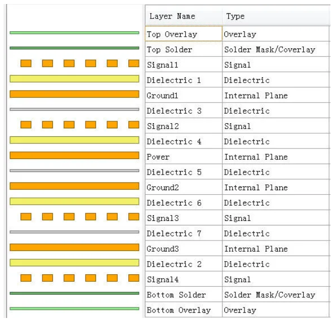
Next, the software generates an 8-layer PCB according to the requirements of the above figure. We can see that in addition to the 8 layers we designed, the PCB has other layers 1, Top , , Top Paste, Paste, Top , , Drill Guide, Keep-Out Layer, Drill , Multi-Layer, we will introduce them respectively below:
: Signal layer.
: formation.
Power: power layer.
1: The mechanical layer is generally used to place indicative information about board manufacturing and assembly methods, such as PCB dimensions, size marks, data files, via information, assembly instructions, and other information.
Top: The top silk screen layer, which is used to mark the projected outline of the top-layer components, the label, nominal value or model of the components, and various comment characters. After the PCB production is completed, it will be displayed on the top layer.
: Bottom screen printing layer, which is used to mark the projected outline of bottom components, component labels, nominal values or models, and various comment characters, which will be displayed on the bottom layer after PCB production is completed.
Top Paste: The top layer of solder paste protection layer, which means that this layer is used for stencil, and is used for surface mounting the top chip. A simple understanding means that only the pads of the chip mounted on the top layer of the PCB will be displayed on this layer, and nothing else will be displayed on this layer (such as vias, through-hole pads).
Paste: The underlying solder paste protective layer, which is also used as a stencil for surface mounting of the underlying chip. Only the pads of the chips on the bottom surface of the PCB will be displayed on this layer, and nothing else will be displayed on this layer (such as through-hole 8-layer circuit board production , through-hole pads).
Top: The top solder mask layer. In layman's terms, what you see on this layer is all exposed copper after the PCB is produced (such as surface mount pads, vias, through hole pads, and places where copper needs to be exposed) , all other parts are covered with oil.
: The bottom solder mask layer, the explanation is the same as above.
Drill Guide: PCB drilling guide layer, drawing drilling diagrams, used for documents.
Keep-Out Layer: Disable the wiring layer, used to set the electrical boundary
Drill: PCB drilling position layer 8-layer circuit board production , giving the drilling position, used for files.
Multi-Layer: This layer shows PCB components that span multiple layers, such as pads for vias, vias, etc.
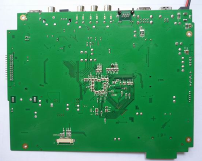
In fact, for our users, the commonly used layers in design are signal layer, power layer, ground layer, silk screen layer, and mechanical layer. Other layers are of little concern unless specifically designed.
Comment on this article here
-
No comment

Ripple
Hi everyone, I'm Ripple, Sales Director of KFPCBA Tech Ltd. If you are looking for a one-stop PCB and PCB assembly manufacturer in China, KFPCBA is your best choice! Please feel free to contact our team! Thanks!
Contact me now


