


 tel:+86-18825224069
 email:
 address:201, Factory 6, Longhui Industrial Park, Fuqiao 3rd District, Xinhe Community, Fuhai Street, Baoan District, Shenzhen china
PCB Board production Process And Information Introduction
Release date:2022-11-28 14:51:56 Number of views:103
PCB Board production Process And Information Introduction
I. Overview
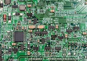
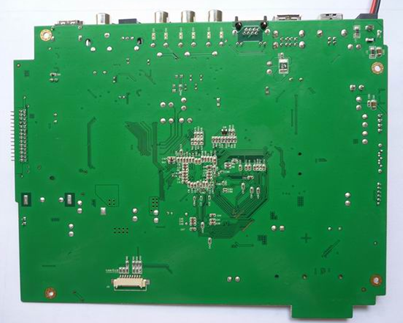
Printed circuit board (board referred to as PCB) is to concentrate the connection of ordinary electronic circuit components on a substrate, thereby improving reliability and wiring density, and also serving as the physical carrier of electronic components.
The PCB board is generally composed of a conductor layer () and an insulating layer (), and each conductor layer is electrically connected through the usual metal hole (Via hole). According to the number of conductor layers, PCB can be divided into single-sided (-side), double-sided (-side) and multi-layer () boards.
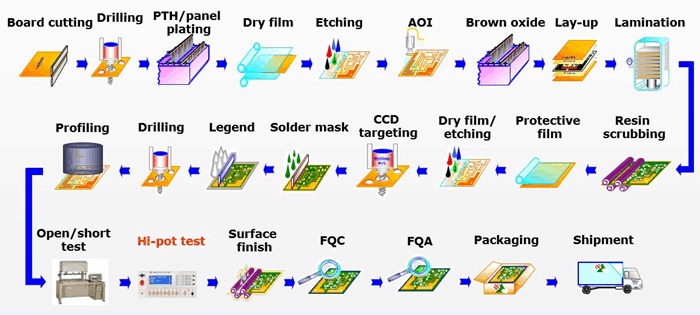
PCB circuit board production process
2. Basic process
Single panel: cutting ()→drilling () or beer hole ()→D/F→etching ()→green oil (S/M)→white (C/M)→surface treatment→forming ()→ET → FQC → Packing () → Shipment
Double-sided panel: cutting → drilling → PTH → panel (Panel) → D/F → graphic ( ) → etching → post-single-sided process
Multi-layer board: cutting → inner circuit (Inner D/F) → Brown oxide → pressing () → molding (Inner) → the same double-panel process
Water gold board process: material cutting→drilling→PTH→board electricity→water gold copper plating+nickel gold plating→etching board→after the same double-sided board process
3. Process introduction
1. Inner line
Process purpose: to form circuit graphics for each inner layer before lamination.
The basic process is: internal D/F → etching → film removal
2. Browning
Purpose of the process: to form a microscopically rough surface on the copper surface of the circuit diagram.
The basic process is: pretreatment→browning→dry board
3. Lamination
Purpose of the process: Laminate conductive layers and insulators into semi-finished products that meet MI requirements
Basic process: pre-processing→stacking→pressing→folding→forming
4. Drilling
Process purpose: to form a certain size and number of through holes or blind holes on the board
Basic process: Drill belt inspection → upper board → trial drilling → first inspection → drilling → inspection
Drilling method: a. Mechanical drilling
b. Laser drilling
5. Immersion Copper
The purpose of the process: to deposit a layer of 0.3-0.5um copper on the hole wall through a chemical reaction, so that the hole wall has conductivity. It is also called electroless copper plating and hole metallization.
Basic process: Coarse grinding → (remove slag) → degreasing → micro-etching → pre-soaking → activation → acceleration → copper cylinder → plate electric → fine grinding → copper inspection
6.D/F
Purpose of the process: transfer the circuit diagram line to the copper surface
Basic process: Grinding → Film → Exposure → Development → Leakage
7. Graphic plating
Process purpose:
a. Thicken the copper plating layer in the hole to ensure good conduction and high reliability;
b. Plating resist layer to prepare for subsequent etching process.
Basic process: pre-treatment → copper plating → tin plating → lower plate → fried sticks
8. Etching
The purpose of the process: to etch away the excess copper layer, and then form the circuit pattern required by the customer
Basic process: D/F stripping→etching→tin stripping→etching inspection Immersion Ni-gold plate needs via hole treatment and immersion before etching
9. Green Oil
The purpose of the process: a. Make the circuit board form a solder mask layer
b. Prevent the copper oxidation of the line
Basic process: pre-processing → screen printing → pre-baking → exposure → development → curing → green inspection
Waterfall method: a. Screen printing
b. Cord coating
c. Electrostatic spraying
10. White characters
Purpose of the process: use heat-curable white ink to print symbols representing each component at the corresponding position on the surface of the W/F PCB board, so that the insertion and placement of components can be clearly marked, and it is convenient to insert and mount components to avoid wrong installation and leakage. Pack.
Basic process: board entry→oiling→silk printing→curing→inspection
C/M process type: a, white silk screen printing
b. Blue glue screen printing
c, carbon oil screen printing
11. Surface treatment
The purpose of the process: to cover the surface of the holes and pads of the plug-in and patch with a layer of solderable plating or coating to prevent the oxidation of the copper surface and protect the solderability.
Surface treatment type (factory):
a, HASL, also known as hot air leveling (HAL)
b. Immersion nickel gold, also known as nickel gold (ENIG)
c. Immersion Silver (Ag)
e, anti-oxidation, also known as OSP
Introduction of various surface treatments
Thick gold plating (including G/F plating)
The process of thick gold plating is different from other surface treatments. The position of thick gold plating is generally not used as a welding basis, but as a plug connection interface, which requires high wear resistance and corrosion resistance, and has a certain hardness. .
Basic process: pre-treatment → nickel-plated gold → gold-plated
The G/F plating process also includes blue glue and flying wing grinding wheel grinding steps, and some thick gold plating also includes the second D/F process.
Hallet tin
Basic process: pre-treatment→preheating→passing rosin→spraying tin→spraying tin→washing plate→inspection (for spray tin plate with G/F, red glue is required before HAL→cold reel→baked plate→hot reel step)
Immersion Nickel Gold
Basic process: grinding plate→pretreatment→pre-soaking→activation→immersion nickel→immersion gold→anti-oxidation→dry plate→inspection
Immersion tin
Basic process: Grinding board→Pretreatment→Low temperature tin→High temperature tin→Alkaline washing→Water washing→Dry board→Inspection
The general process of immersion tin plate is to immerse tin after forming
Antioxidant
Basic process: pre-treatment → anti-oxidation immersion → dry plate → inspection
The anti-oxidation process is anti-oxidation after molding
Gold-plated surface
Basic process: pretreatment→copper plating→nickel plating→gold plating→etching plate→inspection
12. Molding
Purpose of the process: use mechanical action to process the board into the dimensions required by the customer.
Type: a, beer board
b. Gong board
A. Beer board process: beer mold inspection → mold installation → beer test → first inspection → beer board → edge grinding → board washing
B. Gong plate process: gong belt inspection → plate loading → gong test → first inspection → gong plate → washing plate
13.ET
Purpose of the process: Check whether the electrical performance of the PCB board meets the customer's requirements.
Type: a, OPEN/Short test
b. Impedance test
14. FQC
Purpose of the process: final inspection of the appearance of the product , circuit board production , to prevent leakage of defective products to the customer
15. Packaging
Process purpose: According to the storage and transportation of different types of boards for different customers, it is required to use different materials and different methods for packaging circuit board production , so as to protect and maintain the original properties of PCB to the greatest extent.
Basic process: sub-board → packing → boxing → packing
Comment on this article here
-
No comment

Ripple
Hi everyone, I'm Ripple, Sales Director of KFPCBA Tech Ltd. If you are looking for a one-stop PCB and PCB assembly manufacturer in China, KFPCBA is your best choice! Please feel free to contact our team! Thanks!
Contact me now
Relevant content you may be interested in
Related articles


