


 tel:+86-18825224069
 email:
 address:201, Factory 6, Longhui Industrial Park, Fuqiao 3rd District, Xinhe Community, Fuhai Street, Baoan District, Shenzhen china
Design For PCB Surface Components Considered When Designing PCB Boards
Release date:2022-12-06 15:23:35 Number of views:95
What are the design requirements for PCB surface components to be considered when designing PCB boards?

In order to improve the efficiency of chip processing, when chip processing factories generally process PCBA for customers, they will require customers to make panel design for PCB in the front-end PCB design , so what should be paid attention to in PCB panel design? What are the design requirements for PCB puzzles?
1. The design principle of PCB panel is to optimize the quality of PCB base material, the lowest production cost, the highest production efficiency, and the highest utilization rate of PCB board. In order to improve the efficiency of SMT patch processing, when the size of the PCB is too small, it should be designed as a jigsaw method, and the jigsaw method should also be used for the shape of the special-shaped board PCB.
2. The size of the PCB panel should meet the equipment size requirements of the SMT patch processing production line, which is conducive to SMT patch processing, and the panel size should be determined according to the thickness of the PCB board.
3. The frame (clamping side) of the PCB panel should adopt a closed-loop control design scheme to ensure that the PCB panel is fixed and not easily deformed after being placed on the fixture.
4. The appearance design of the PCB splicing method is as close to the square as possible. It is strongly recommended to use the 2×2 or 3×3 splicing method for pcb processing , and do not combine male and female boards if it is not necessary;
5. The dividing groove between the panels should meet the flatness requirements of the surface during PCBA patch processing.
6. There are mainly three interconnection methods between the small PCBs in the jigsaw puzzle: broken label type, double-sided V-shaped groove and stamp plate type. The design should take into account the mechanical strength and flatness of the surface, as well as the ease of division of subsequent finished product assembly.
7. The layout of PCB surface components should be considered when designing PCB boards, especially the direction of wave soldering. When processing double-sided patches, double-number jigsaw panels, half front and back sides, and identical graphics on both sides can be used. This design can use the same stencil, saving production preparation time, improving production efficiency and equipment utilization.
8. In PCB panel design, the arrangement of components should avoid splitting stress and cause component cracks. The use of pre-scored panel structure can minimize warping and deformation during board separation, and reduce the stress on components. To a minimum, try not to place valuable components next to the process side.
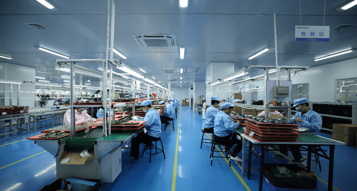
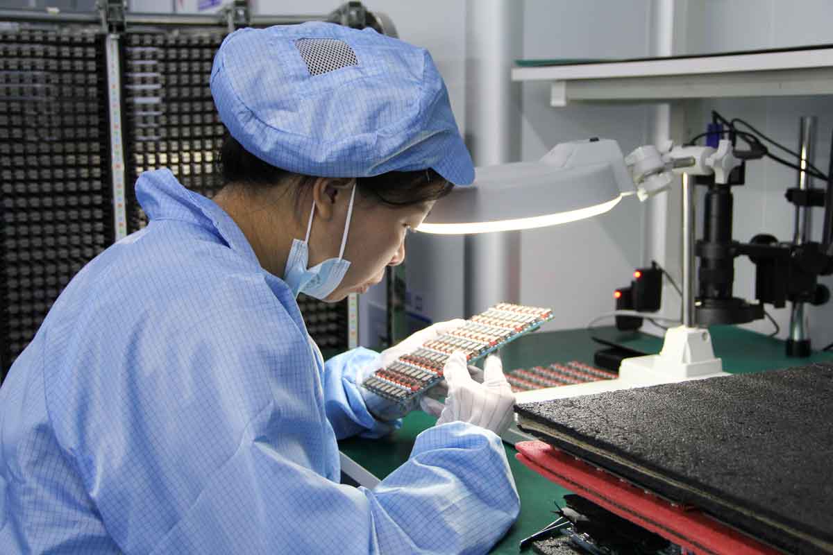
The above content is the technology shared by KFPCBA, a Shenzhen SMT patch processing factory. I hope it will be helpful to you. To learn more about SMT patch processing knowledge and pcb processing , welcome to pay attention to KFPCBA.
Comment on this article here
-
No comment

Ripple
Hi everyone, I'm Ripple, Sales Director of KFPCBA Tech Ltd. If you are looking for a one-stop PCB and PCB assembly manufacturer in China, KFPCBA is your best choice! Please feel free to contact our team! Thanks!
Contact me now


