


 tel:+86-18825224069
 email:
 address:201, Factory 6, Longhui Industrial Park, Fuqiao 3rd District, Xinhe Community, Fuhai Street, Baoan District, Shenzhen china
PCB Design Method and Technical Hierarchy
Release date:2022-12-15 16:18:17 Number of views:134
The design method of the printed circuit board and the hierarchical composition of the technical board
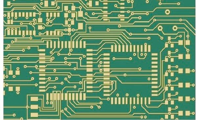
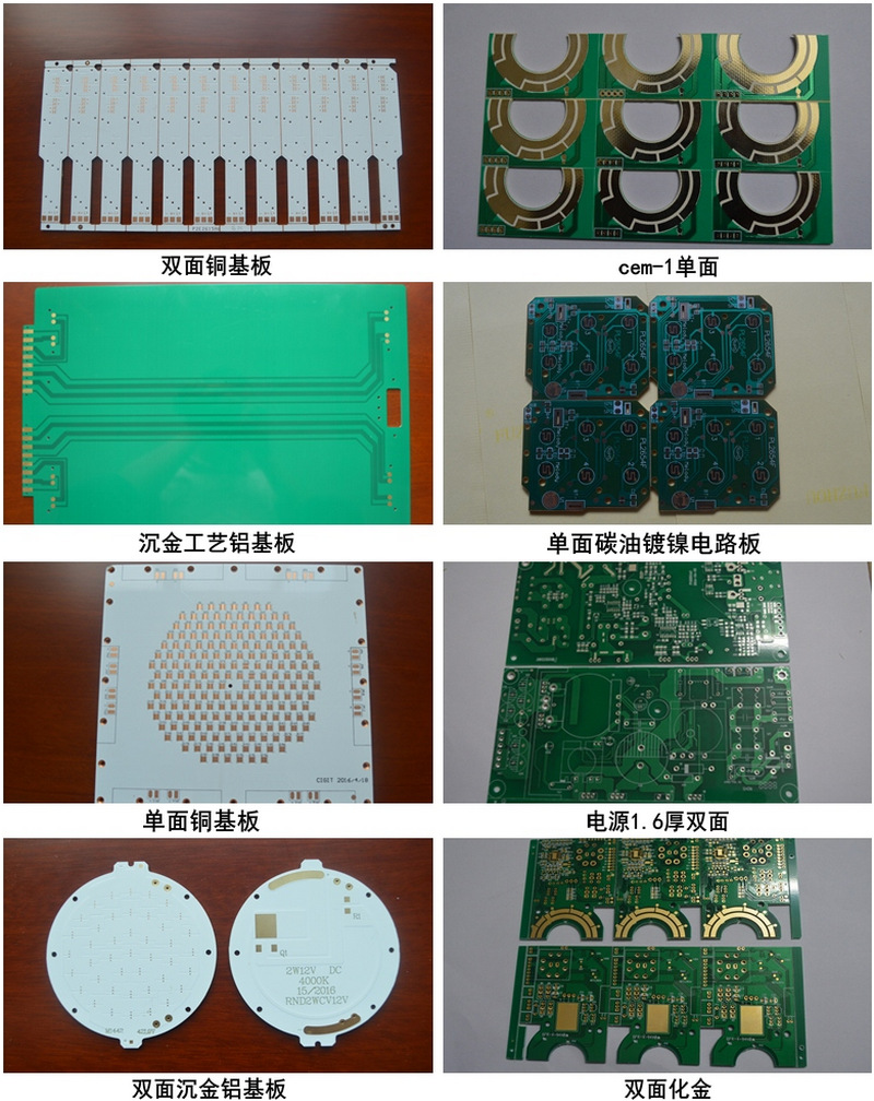
The layer composition of the actual printed circuit board: copper foil layer, printed material layer, silk screen layer. The copper foil layer includes the signal layer and the internal electrical layer in the software design, and mainly completes the electrical connection characteristics of the circuit. The number of layers of copper foil is usually defined as the number of layers of printed circuit boards (single panel, double panel, multilayer board). The printed material layer is also called an insulating layer or a copper clad laminate. Its main function is to isolate the power layer and the wiring layer and support the entire printed circuit board. The silk screen layer is located on the top layer of the printed board to protect the copper foil layer and record some logo patterns and text symbols (usually white), which is convenient for installation and repair.
Design Methods and Skills of Printed Circuit Board
The layer selection of printed circuit boards should be considered in terms of electrical performance, reliability, processing technology requirements and economic indicators. Commonly used copper clad laminates are: phenolic paper laminates, epoxy paper laminates, polyester glass cloth laminates, epoxy glass cloth laminates. Epoxy paper laminates are generally used in laboratories. It is best to use polyester glass cloth laminated boards for UHF printed circuit boards. For electronic equipment that requires flame retardancy, laminated flame-retardant printed circuit boards impregnated with flame-retardant resins are also required. The thickness of the printed circuit board should be determined according to the function of the printed circuit board, the weight of the installed components, the size of the printed circuit board socket, the dimensions of the printed circuit board and the mechanical load it bears. First of all, sufficient rigidity and strength should be ensured. Common printed circuit board thicknesses are 0.5mm, 1.0mm, 1.5mm, and 2.0mm.
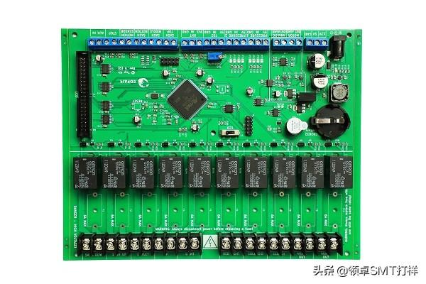
Mainly based on manual layout, generally follow the following rules:
1) Layout according to the function of the circuit: As far as possible, the components are laid out according to the schematic diagram and the circuit board is customized . The signal enters from the left and outputs from the right, and enters from the top and outputs from the bottom. According to the circuit flow, arrange the position of each functional circuit unit to keep the signal flowing smoothly and in the same direction.
2) Layout around the central circuit: the arrangement of components should be uniform, regular and compact. The digital circuit part should be separated from the analog circuit part.
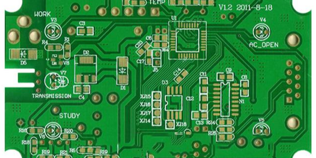
3) The shorter the connection between high-frequency components, the better to reduce electromagnetic interference; components that are susceptible to interference should not be too close , and components with high potential differences should meet the specified safety requirements.
4) The adjustable components are placed on the printed circuit board at a position that is easy to adjust; if it is adjusted outside the machine, its position should correspond to the position of the adjustment knob on the chassis panel; the distance between the component and the edge of the printed circuit board should be more than 3mm . Components with too much weight should not be installed on printed circuit boards; heating components should be kept away from heat-sensitive components.
5) The order of component placement: first place components with a fixed orientation that closely match the structure. For example, power sockets, indicator lights, switches and connecting plug-ins, etc.; then place special components, such as heating elements, transformers, integrated circuits, etc.; finally place small components, such as resistors, capacitor diodes, etc.
The above is what are the skills of printed circuit boards? The introduction of the design methods and skills of printed circuit boards, I hope it can help everyone, and if you want to know more information about printed circuit boards, you can pay attention to the update of KFPCBA .
Comment on this article here
-
No comment

Ripple
Hi everyone, I'm Ripple, Sales Director of KFPCBA Tech Ltd. If you are looking for a one-stop PCB and PCB assembly manufacturer in China, KFPCBA is your best choice! Please feel free to contact our team! Thanks!
Contact me now
Relevant content you may be interested in
Related articles


