


 tel:+86-18825224069
 email:
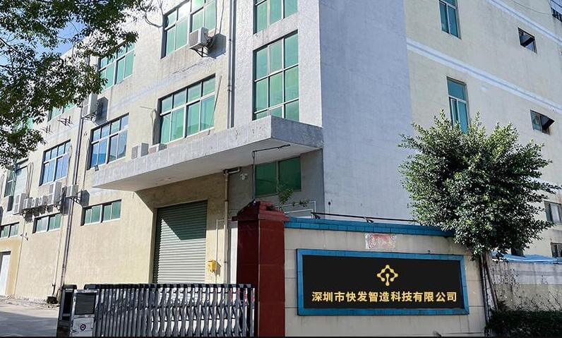
 address:201, Factory 6, Longhui Industrial Park, Fuqiao 3rd District, Xinhe Community, Fuhai Street, Baoan District, Shenzhen china
How Is The Large Size PCB Board Made?
Release date:2022-12-15 16:45:40 Number of views:88
How is the large size PCB board made?
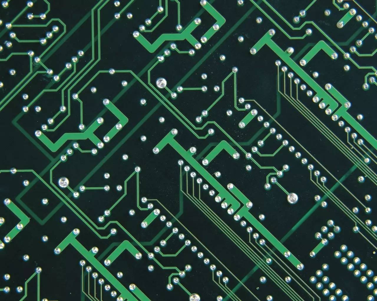
In recent years, 5G is becoming an important driving force for the digital transformation of the manufacturing industry. Its basic equipment uses super-sized PCBs, which can greatly improve the printing pass-through rate and ensure the quality of signal transmission. However, ultra-large PCBs are the limit of current SMT equipment processing capabilities, and the superposition of large board and stencil processing tolerances leads to solder paste printing problems, which poses a great challenge to production and has always been a difficulty that the industry needs to solve urgently.
Because the company's product development has launched a circuit board that requires a large size for testing, but many PCB factories have been found, but they are all rejected on the grounds that they do not have this production process or cannot produce it.
Nowadays, customers in the fields of light box light bar, rail traffic control system, high-definition audio and video controller, medical equipment, aerospace and industrial control are quite common in the application of large-size circuit boards . Therefore, customers in these fields urgently need a factory that can solve production problems.
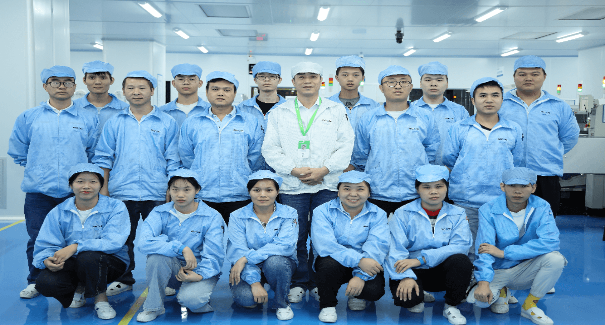
As a circuit board factory focusing on high-end PCBs , KFPCBA has provided customized services for many well-known companies.
How is the large size PCB board made?
1. Separate equipment is required. Due to size limitations, large-size PCBs cannot be operated on conventional equipment, so large-size equipment needs to be purchased separately, so the cost becomes higher, but how the market is a risk of customized processing of circuit boards, most manufacturers are unwilling to take risks .
2. The board is easily damaged. The area of a large-size board is usually several to dozens of times larger than that of a conventional board. If the size is too large, the board is easily damaged, and problems such as board bending and warping are prone to occur during processing, and the cost of the board is greatly increased.
3. High process requirements. Due to the special performance of the large-size board, there are huge differences in its design parameters and some requirements that need to be met compared with the conventional PCB board. The technology involves a wider range of circuit board custom processing , and the production is more difficult.
4. There are more than 20,000 devices on a single PCB, involving different packages, and the amount of solder paste required by each device is uneven;
Therefore, most manufacturers would rather take some regular orders to reduce cost losses, but what the KFPCBAs need to do is the difficulty board, fight for quality, and workmanship!
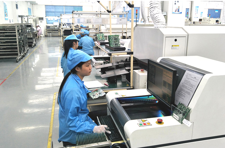
Large size board
How does KFPCBA ensure the production of high-quality and large-size PCBs?
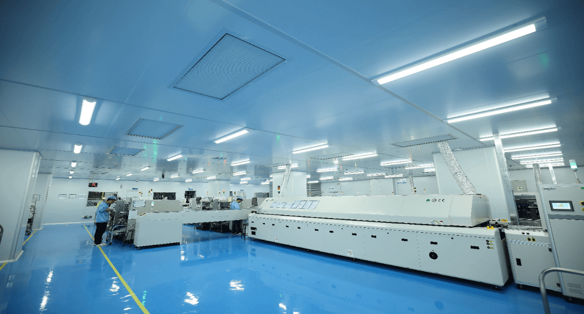
KFPCBA has newly invested in a batch of special equipment for ultra-long boards, such as: custom six-axis drilling rigs, custom plug hole screen printing machines, special CNC gong machines, custom flying probe machines, and 12,000-point super-large tabletop testing machines, etc.; the second best material determines For the continuous stability of large-size products in production and customer use, the KFPCBA uses KB A-grade boards to meet the stable expansion and contraction coefficient and board water absorption rate, avoiding quality problems such as board deformation, and providing customers with consistent placement and products. Performance and stability are guaranteed; and KFPCBA has independently developed a set of production processes and parameters for large-scale orders to ensure quality and delivery.
Large size board details
KFPCBA is committed to providing customers with multi-layer board large-size special process customization services to solve the problems of enterprise multi-layer board production. Users are welcome to come to consult.
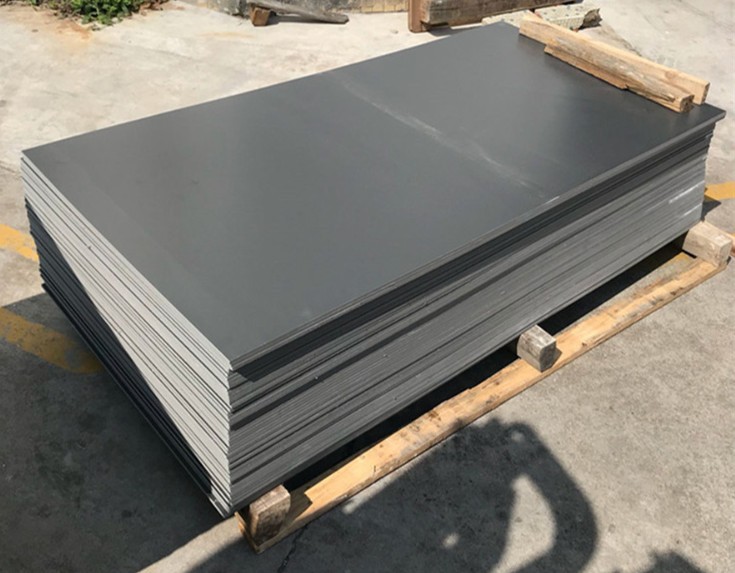
Custom Craft KFPCBA
1. Support 1-14 layers of small and medium batch orders, and consult customer service for more layers;
2. Can do HDI blind buried hole process;
3. The board uses Kingboard A-grade board (KB-6164), which can be used as a halogen-free board;
4. The maximum size can be one meter;
5. Pink, transparent, purple and other ink colors;
6. Support copper thickness 10oz, hole copper 35μm;
7. Lamination structure can be customized for multi-layer boards;
8. Support multi-level impedance matching;
9. Copper-clad board edge, two-color ink, socket hole, countersunk hole, square groove, stepped hole, stepped groove, nickel-palladium-gold and other special processes;
10. PCBA can be pasted in one set, and can be pasted on both sides;
Comment on this article here
-
No comment

Ripple
Hi everyone, I'm Ripple, Sales Director of KFPCBA Tech Ltd. If you are looking for a one-stop PCB and PCB assembly manufacturer in China, KFPCBA is your best choice! Please feel free to contact our team! Thanks!
Contact me now


