 address:201, Factory 6, Longhui Industrial Park, Fuqiao 3rd District, Xinhe Community, Fuhai Street, Baoan District, Shenzhen china
What Processing Methods Of A Flexible Circuit Board
What are the processing methods of a flexible circuit board? -Shenzhen KFPCBA
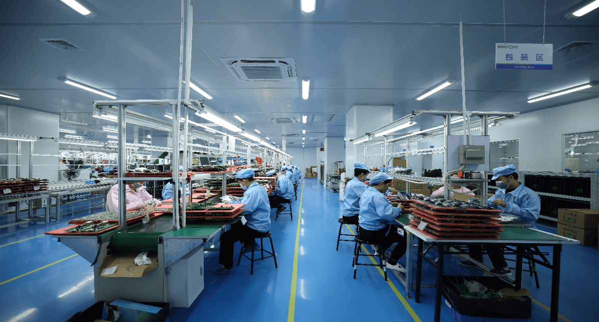
The invention relates to the technical field of circuit boards, in particular to a processing method of flexible circuit boards.
Background technique:
Flexible circuit boards, also known as flexible circuit boards and flexible circuit boards, are highly sought after for their light weight, thin thickness, and free bending and folding. With the rapid development of the electronics industry, circuit board design is becoming more and more High-precision, high-density, flexible circuit board is a technology developed by the United Kingdom in the 1970s for the development of aerospace technology. It is a kind of high reliability and excellent performance made of polyester film or copolymer. Flexible color printed circuit, by embedding the circuit design on the flexible thin plastic sheet, so that a large number of precision devices can be stacked in a narrow and limited space, and then a flexible circuit can be produced. In the structure of the flexible circuit, the composition The materials used are insulating films, conductors and adhesives, and traditional flexible circuit boards are not waterproof, and the heat dissipation capacity is average. There are certain limitations in the actual use of flexible circuit boards. Therefore, we propose a processing method for flexible circuit boards. Way.
Technical realization elements:
The main purpose of the present invention is to provide a processing method of a flexible circuit board, which can effectively solve the problems in the background technology.
In order to achieve the above object, the technical scheme that the present invention takes is:
A processing method for a flexible circuit board, comprising the following steps:
s1. Cutting the material. Preliminary cutting of the base material. The purpose of this is to reduce the excess waste as much as possible. When cutting the material, if the cutting is large, it will also promote the excess material to cause waste;
s2. Copper foil pressing. The base material is sandwiched between two brass sheets by the machine. Firstly, the long circular sheets are cut uniformly, and then separated with a laminate to form a stack, and then sent into the vacuum pump box to place the tight armatures of each layer in the At the same time, it is sent to a low-temperature and high-pressure box for processing, because the polymer film located in the middle layer itself has a coating of heat-activated adhesive, so that the original three layers will be bonded into a whole;
s3. Drill positioning holes and thermal blind holes, and drill positioning holes and thermal blind holes on the base plate through a drilling machine;
s4, film, stick the fourth layer of photosensitive layer film on the surface of the circuit board through the film adding machine;
s5. Exposure, use a notebook to draw the integrated circuit diagram according to the customer's needs, and then put the board into the exposure machine, and the notebook will control the machine to perform laser scanning on the photosensitive layer;
s6. Acidic etching, alkaline ammonia water is used to dissolve and etch the exposed copper surface, that is to say, to remove the copper surface not covered by the film, the surface of the irradiated photosensitive layer will react and harden, which can protect the lower surface. The copper layer is not pickled;
s7. Paste the insulating layer. After the pickling machine cleans the area that has not been irradiated by the laser, the remaining copper layer is the integrated circuit drawn in the original notebook, so that the fifth insulating layer is placed on the circuit board for rapid processing , and finally the entire circuit The boards are separated by plastic paper and laminated boards and put into a stack, and then sent to the vacuum pump box to tightly arm the layers together, and then sent to the low-temperature and high-pressure box for processing;
s8. Pressing, wait until the circuit board is cooled, manually put it into the mold, and press the circuit board with a pressing machine;
s9, spraying the waterproof coating, coating the nano-waterproof coating on the surface of the circuit board by a coating machine, and drying;
s10. Inkjet color printing characters, save brick color printing characters through inkjet printing;
s11, punching, cutting by cutting device, a flexible circuit board is about to be completed;
s12. Inspection, inspecting the finished circuit board.
Preferably, in the step s5, the minimum negative-to-negative difference ratio of sensitivity is 3:1, the ratio of sodium carbonate in the exposure fixer reaches 1.5-2%, and stays for at least 15-30 minutes after exposure.
Preferably, in the step s6, alkaline lye such as sulfuric acid or nitric acid is used for the soft board, but ammonia water such as dichloromethane is used when etching the hard circuit.
Preferably, in the step s7, the low-temperature and high-pressure oven treatment is carried out at 120-130 degrees for about 1-2 hours.
Preferably, in the step s7, the dirt on the surface of the circuit board is removed by a sticky roller, and then a fifth insulating layer is placed.
Preferably, in the step s11, the circuit board is tested by using a flying probe or a bed of needles, and the test is mainly a leakage test.
Compared with the prior art, the present invention has the following beneficial curative effects: by coating the waterproof coating, a transparent and colorless molecular water-resistant film chain can be produced in water and on the circuit board normally, making it difficult for water to touch the circuit board, So as to achieve a certain waterproof effect and improve the service life;
By reasonably controlling the exposure time and adjusting the ratio of yin and yang differences in sensitivity, it is possible to prevent poor image resolution and scattered light and reflected light from reaching the film cover;
Through the thermal blind holes, the thermal blind holes can effectively reduce the junction temperature of the circuit board, improve the uniformity of the water temperature in the length direction of the single board, and provide the possibility to adopt other heat dissipation methods on the reverse side of the circuit board.
Description of drawings
FIG. 1 is a schematic diagram of a process flow of a processing method of a flexible circuit board according to the present invention.
Specific implementation method
In order to make the technical means realized by the present invention, creation features, goals and effects easy to be understood, the following will further explore the present invention in conjunction with specific implementation methods.
Example 1
A processing method of a flexible circuit board as shown in Figure 1 includes the following steps:
s1. Cutting the material. Preliminary cutting of the base material. The purpose of this is to reduce the excess waste as much as possible. When cutting the material, if the cutting is large, it will also promote the excess material to cause waste;
s2. Copper foil pressing. The base material is sandwiched between two brass sheets by the machine. Firstly, the long circular sheets are cut uniformly, and then separated with a laminate to form a stack, and then sent into the vacuum pump box to place the tight armatures of each layer in the At the same time, it is sent to a low-temperature and high-pressure box for processing, because the polymer film located in the middle layer itself has a coating of heat-activated adhesive, so that the original three layers will be bonded into a whole;
s3. Drill positioning holes and thermal blind holes, and drill positioning holes and thermal blind holes on the base plate through a drilling machine;
s4, film, stick the fourth layer of photosensitive layer film on the surface of the circuit board through the film adding machine;
s5. Exposure, use a notebook to draw the integrated circuit diagram according to the customer's needs, and then put the board into the exposure machine, and the notebook will control the machine to perform laser scanning on the photosensitive layer;
s6. Acidic etching, alkaline ammonia water is used to dissolve and etch the exposed copper surface, that is to say, to remove the copper surface not covered by the film, the surface of the irradiated photosensitive layer will react and harden, which can protect the lower surface. The copper layer is not pickled;
s7. Paste the insulating layer. After the pickling machine cleans the area that has not been irradiated by the laser, the remaining copper layer is the integrated circuit drawn in the original notebook, so the fifth insulating layer is placed, and finally the entire circuit board is covered with plastic The paper and the laminated boards are separated and put into a stack, and then sent to the vacuum pump box to tightly arm the layers together, and then sent to the low-temperature and high-pressure box for processing;
s8. Pressing, wait until the circuit board is cooled, manually put it into the mold, and press the circuit board with a pressing machine;
s9, spraying the waterproof coating, coating the nano-waterproof coating on the surface of the circuit board by a coating machine, and drying;
s10. Inkjet color printing characters, save brick color printing characters through inkjet printing;
s11, punching, cutting by cutting device, a flexible circuit board is about to be completed;
s12. Inspection, inspecting the finished circuit board;
In step s5, the minimum negative-to-negative difference ratio of sensitivity is 3:1, the ratio of sodium carbonate in the exposure fixer reaches 1.5-2%, and stays for at least 15-30 minutes after exposure; in step s6, sulfuric acid is used for the soft board Or alkaline lye such as nitric acid, but use lye such as dichloromethane when etching hard circuits; in step s7, the low-temperature and high-pressure box is processed with 120-130 degree baking for about 1-2 hours; step In s7, the dust on the surface of the circuit board is removed by the sticky roller, and then the fifth layer of insulation is placed.
It should be noted that the present invention is a processing method for flexible circuit boards, and the base material is initially cut. The purpose of this is to reduce unnecessary waste as much as possible. Excess material leads to waste. The base material is sandwiched between two brass sheets by the machine. First, the long circular sheets are cut uniformly, and then they are separated by laminates and placed in a stack, and then sent into the vacuum pump box to tighten the layers together. Then send it to a low-temperature and high-pressure box for processing, because the polymer film located in the middle layer itself has a coating of heat-activated adhesive, so that the original three layers will be bonded into a whole, and the positioning is drilled on the substrate board by a drilling machine Holes and thermal blind holes are positioned through the positioning holes, and the thermal blind holes can effectively reduce the junction temperature of the circuit board, improve the uniformity of the water temperature in the length direction of the board, and provide the possibility to adopt other heat dissipation methods on the reverse side of the circuit board. The machine sticks the fourth layer of photosensitive layer film on the surface of the circuit board, draws the integrated circuit diagram with a notebook according to the customer's needs, and then puts the board into the exposure machine, the notebook will control the machine to scan the photosensitive layer with laser, and alkaline ammonia water will dissolve the engraving Etch the exposed copper surface, that is to say, remove the copper surface that is not covered by the film. The surface of the irradiated photosensitive layer will react and harden, which can protect the underlying copper layer from being pickled, and the pickling machine is not cleaned. After the area irradiated by the laser, the remaining copper layer is the integrated circuit drawn in the original notebook, so the fifth insulating layer is placed, and finally the entire circuit board is separated by plastic paper and laminated boards and placed in a stack. Send it into the vacuum pump box to make the layers of the armature tightly together, and then send it into the low-temperature and high-pressure box for processing. After the circuit board cools down, put it into the abrasive tool manually, press the circuit board with a pressing machine, and pass the coating machine on the circuit board. The surface of the board is coated with a nano-waterproof coating and dried, and the characters are printed by inkjet printing and color printing, and then cut by a cutting device. A flexible circuit board is about to be completed, and finally the finished circuit board is inspected.
In fact, the above implementation examples are only examples for clearly explaining, rather than limiting the implementation method. For those skilled in the art, on the basis of the above description, other changes or changes in different ways can also be made. It is not necessary and impossible to give an exhaustive list of all implementation methods here. However, the obvious changes or variations derived therefrom are still within the scope of protection of the present invention.
Technical Features:
1. A processing method for a flexible circuit board is characterized in that it comprises the following steps:
s1. Cutting the material. Preliminary cutting of the base material. The purpose of this is to reduce the excess waste as much as possible. When cutting the material, if the cutting is large, it will also promote the excess material to cause waste;
s2. Copper foil pressing. The base material is sandwiched between two brass sheets by the machine. Firstly, the long circular sheets are cut uniformly, and then separated with a laminate to form a stack, and then sent into the vacuum pump box to place the tight armatures of each layer in the At the same time, it is sent to a low-temperature and high-pressure box for processing, because the polymer film located in the middle layer itself has a coating of heat-activated adhesive, so that the original three layers will be bonded into a whole;
s3. Drill positioning holes and thermal blind holes, and drill positioning holes and thermal blind holes on the base plate through a drilling machine;
s4, film, stick the fourth layer of photosensitive layer film on the surface of the circuit board through the film adding machine;
s5. Exposure, use a notebook to draw the integrated circuit diagram according to the customer's needs, and then put the board into the exposure machine, and the notebook will control the machine to perform laser scanning on the photosensitive layer;
s6. Acidic etching, alkaline ammonia water is used to dissolve and etch the exposed copper surface, that is to say, to remove the copper surface not covered by the film, the surface of the irradiated photosensitive layer will react and harden, which can protect the lower surface. The copper layer is not pickled;
s7. Paste the insulating layer. After the pickling machine cleans the area that has not been irradiated by the laser , the circuit board is quickly processed . The remaining copper layer is the integrated circuit sketched in the original notebook, so the fifth insulating layer is placed, and finally the entire circuit The boards are separated by plastic paper and laminated boards and put into a stack, and then sent to the vacuum pump box to tightly arm the layers together, and then sent to the low-temperature and high-pressure box for processing;
s8. Pressing, wait until the circuit board is cooled, manually put it into the mold, and press the circuit board with a pressing machine;
s9, spraying the waterproof coating, coating the nano-waterproof coating on the surface of the circuit board by a coating machine, and drying;
s10. Inkjet color printing characters, save brick color printing characters through inkjet printing;
s11, punching, cutting by cutting device, a flexible circuit board is about to be completed;
s12. Inspection, inspecting the finished circuit board.
2. According to the processing method of a kind of flexible circuit board described in claim 1, it is characterized in that, in the step s5, the minimum negative-yang differential ratio of sensitivity is 3:1, and the ratio of sodium carbonate of the exposure fixer reaches 1.5- 2%, and stay at least 15 to 30 minutes after the exposure.
3. According to the processing method of a kind of flexible circuit board described in claim 1, it is characterized in that, in the step s6, sulfuric acid or nitric acid and other alkaline lyes are used for the soft board, but when etching the hard circuit The time is to use ammonia such as dichloromethane.
4. The processing method of a flexible circuit board according to claim 1, characterized in that, in the step s7, the low-temperature and high-pressure box is baked at 120-130 degrees for about 1-2 hours.
5. The processing method of a flexible circuit board according to claim 1, characterized in that, in the step s7, the dust on the surface of the circuit board is removed by a sticky roller, and then a fifth insulating layer is placed.
6. The processing method of a flexible circuit board according to claim 1, wherein in the step s11, the circuit board is tested by using a flying probe or a bed of needles, and the test is mainly a leakage test.
Technical summary
The invention discloses a processing method of a flexible circuit board, comprising the following steps: material cutting, copper foil pressing, drilling positioning holes and thermal blind holes, film sticking, exposure, acid etching, insulating layer sticking, pressing, spraying and waterproofing Coating, inkjet color printing characters, die cutting and inspection. The processing method of a flexible circuit board according to the present invention can achieve a transparent and colorless molecular water-resistant film chain in water and on the circuit board normally by coating the waterproof coating, making it difficult for water to touch the circuit board. So as to achieve a certain waterproof effect and improve the service life. By reasonably controlling the exposure time and adjusting the ratio of negative and positive differences in sensitivity, it can prevent poor image resolution and scattered light and reflected light from reaching the film cover. Blind holes and thermal blind holes can effectively reduce the junction temperature of the circuit board, improve the uniformity of the water temperature in the length direction of the board, and provide the possibility to adopt other heat dissipation methods on the reverse side of the circuit board.
-
No comment




 tel:+86-18825224069
 email:


