


 tel:+86-18825224069
 email:
 address:201, Factory 6, Longhui Industrial Park, Fuqiao 3rd District, Xinhe Community, Fuhai Street, Baoan District, Shenzhen china
Soldering Quality Problems And Solutions In Reflow Soldering During Electronic Processing
Release date:2022-12-09 17:00:01 Number of views:138
Soldering quality problems and solutions in reflow soldering during electronic processing

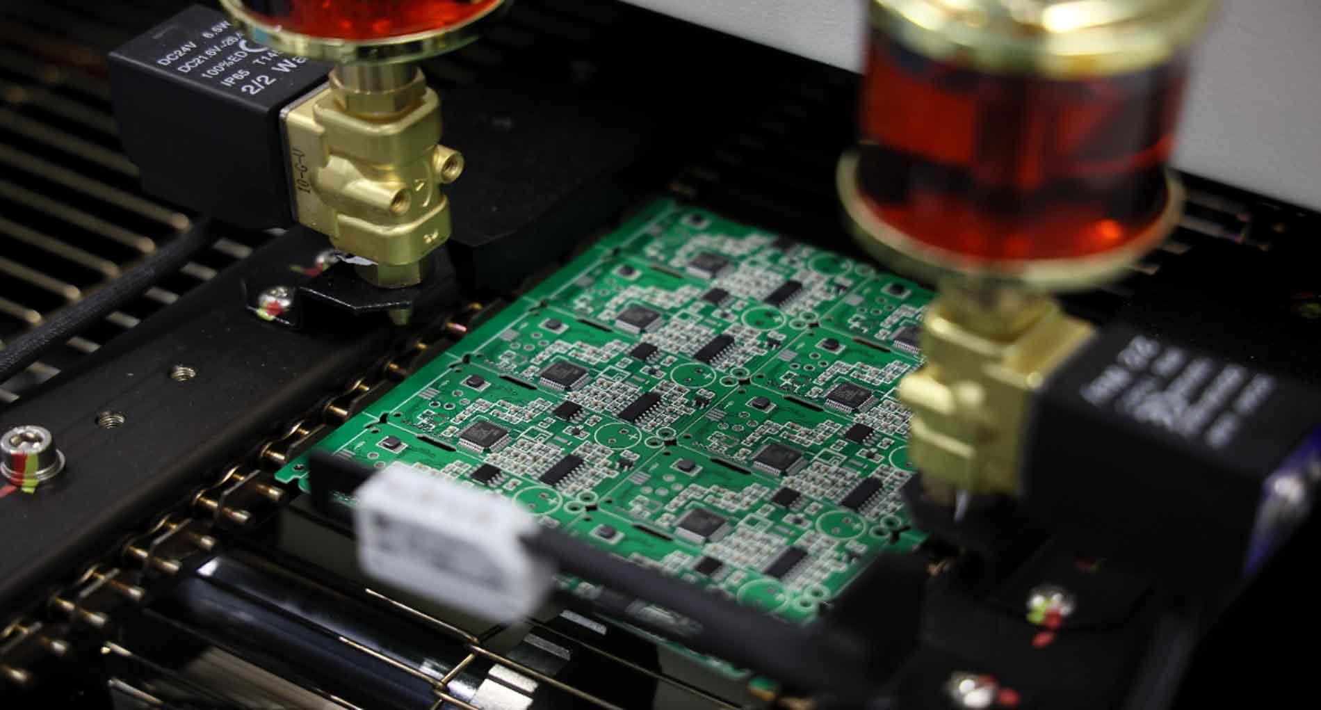
Reflow soldering is a very critical process in SMT chip processing, and the quality of reflow soldering will directly affect the surface mount quality of PCBA processing. If you want to optimize the reflow soldering process to avoid poor processing, you must first understand what factors will affect the quality of reflow soldering. The following professional PCBA foundry materials will briefly introduce you. In the actual electronic processing process, the soldering quality problems of reflow soldering are not only related to the process of reflow soldering, but also may be related to some factors in other PCBA processing processes, such as production line equipment conditions, PCBA substrate pads and Manufacturability design, component solderability, solder paste quality, printed circuit board processing quality and process parameters of each process of SMT chip processing , etc. The processing quality of the SMT patch has an important relationship with the design of the PCBA pad. The pad design of the PCBA substrate can self-correct a small amount of skew during processing. If it is not appropriate, even if the mounting position is accurate, the position of the component may appear. Defects such as offset. 1. The key elements that should be mastered in the design of PCBA substrate pads: According to the analysis of the solder joint structure of various components, in order to ensure the reliability of solder joints, the pad design should meet the following elements:
Symmetry: The pads at both ends are symmetrical to ensure The surface tension of molten solder is balanced.
Pad spacing: ensure the overlapping size of the component end or pin and the pad Hardang.
The remaining size of the pad: the remaining size after the component end or pin overlaps with the pad ensures that the solder joint can form a meniscus.
Pad width: It should be basically consistent with the width of the component end or pin. Little knowledge of SMT patch processing in electronic processing factories. Nanjing Automotive Electronics SMT Plant
In the process of SMT processing in electronic processing factories, sometimes white spots or white spots appear on the PCBA, which is a relatively uncomfortable problem for the quality of PCBA. So what is the reason for this phenomenon? How do we solve it? The following professional SMT patch processing factory Yinghong Technology will give you a brief introduction to the causes and solutions of these white spots or white spots. Reasons:
1. The circuit board is subjected to thermal stress beyond the reasonable processing range.
2. PCBA is impacted by inappropriate mechanical external force, which makes local resin and glass fiber separate , forming white spots.
3. In the process of SMT processing, it is infiltrated by fluorine-containing chemicals, and the glass fiber is etched to form regular white spots.
Solutions:
Control hot air rectification, infrared heat melting, etc. in strict accordance with processing requirements.
Take measures during the SMT process to minimize or reduce the excessive vibration of the machine, thereby reducing the external force of the machine on the PCBA during the process. How much does Shanghai manufacturer smt chip manufacturer smt industry chip processing cost?There will be some common bad phenomena in the OEM of SMT chip processing. These problems affect the processing quality of PCBA processing plants. So how should these bad phenomena in electronic processing be avoided? 1. Poor wetting Poor wetting refers to the fact that the solder and the substrate welding area during the welding process do not generate an intermetallic reaction after infiltration, resulting in missing or less soldering failures. Solution: Choose a suitable welding process, take anti-pollution measures on the surface of the substrate and components, choose the appropriate solder, and set a reasonable welding temperature and time. OEM common problems and solutions for SMT chip processing
2. Bridging The reasons for bridging in SMT chip processing are mostly due to excessive solder or severe edge collapse after solder printing, or the size of the substrate solder area is out of tolerance , mounting offset, etc., when the circuit tends to be miniaturized, the bridging will cause an electrical short circuit and affect the use of the product. Solution:
To prevent poor edge collapse during solder paste printing.
Pay attention to the design requirements of OEM processing when designing the size of the soldering area of the PCB A substrate.
The mounting position of components should be within the specified range.
4. The PCBA substrate wiring gap and the coating accuracy of the solder resist must be strictly required.
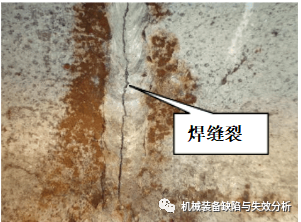
5. Formulate appropriate welding process parameters. 3. When the crack welding PCB just leaves the welding area, due to the difference in thermal expansion between the solder and the joined parts, under the action of rapid cooling or rapid heating, due to the influence of solidification stress or shrinkage stress, SMD will basically produce microcracks. PCB, in the process of punching and transportation, must also reduce the impact stress and bending stress on SMD.
The price calculation of patch processing in the smt industry is currently almost in a transparent stage, and the algorithm for how much it costs per point is very simple. But first of all, the concept of "point" needs to be clarified. Different companies use different algorithms, but most of the key content is still applicable. The main purpose of SMT chip processing is to mount the chip components on the pads of the PCBA substrate. If a pad is calculated as a point, it is only necessary to calculate the number of all pads on the PCB, but when encountering some special components, such as inductors, large capacitors, ICs, etc., additional calculations are required. The specific empirical methods are as follows : For example, the inductance can be counted as 10 points, and the IC is folded in half according to the number of pins. According to the above method, the total number of solder joints of the entire PCBA board in the smt industry can be easily calculated. The next step is to determine the unit price of the solder joints. At present, in the market, the unit price of solder joints varies. From this, it depends on the difficulty of SMT processing and the SMT manufacturer's requirements and capabilities for SMT quality control. Often the price is cheap, there may be no testing link, no material inspection link, it is difficult to guarantee the quality of the entire batch of SMT patches, and there will be great delays in the consistency and reliability of the product. Manufacturers with slightly higher chip prices in the smt industry will have quality control processes and can provide better lead times and services. Customers choose SMT patch suppliers based on their own situation. Which one is better for Foshan smt patch processing? Shanghai Yinghong Electronics!
One thing that is often reused in the maintenance process of SMT patches is the tin strip. The role of the tin strip in PCBA processing is to remove excess solder on the PCBA board. The use of the tin strip is also particular. Below, Yinghong Technology will share with you the method and steps of using the tin strip. Before using the tin strip in SMT processing, it is necessary to dip the front end of the rosin and then approach the solder joint that needs to be removed, and then use a soldering iron to heat and melt the solder joint, and the solder of the solder joint will be sucked away by the tin strip after melting , If it is said that it is not sucked clean, you can repeat the SMT patch factory several times until the patch component can be safely removed. Steps of absorbing solder with tin strip: 1. The width of tin strip used in actual SMT chip maintenance should be reasonably selected according to the solder joints to be removed. 2. Before use, the tin strip needs to be dipped in rosin and kept in good contact with the solder joints to be removed. 3. Put the heated electric soldering iron on the tin-absorbing belt, heat the solder joints to be desoldered by heating the tin-absorbing belt, and wait for the solder to melt. Do not apply pressure to the solder joint during this process, otherwise the components may be damaged and the tip of the soldering iron may be damaged. 4. After all the melted solder is sucked away by the tin-absorbing tape, remove the soldering iron and the tin-absorbing tape, and cut off the saturated part of the solder-absorbing tape, or save it for the next use. 5. Check the solder joints for desoldering. If there is no dryness and coldness, repeat the above steps. If there is more solder in the solder joints, you can use the tip of the soldering iron to take away part of the solder and then use the tin suction tape to absorb it. A brief description of the surface mount IC socket for SMT chip processing. Quotation list for smt patch processing of Hefei inverter motherboard
Brief introduction of solder paste printing machine in SMT electronic processing. Nanjing Automotive Electronics SMT Plant
In the SMT patch processing process of electronic OEM manufacturers, there is a very important processing raw material, that is flux. Flux also occupies a large position in PCBA processing. It is impossible to process high-quality PCBA products with poor-quality flux. As an electronic OEM manufacturer with strict requirements on processing quality, Pater Technology is also in the selection of flux. For those with strict requirements, let me share with you some methods of flux detection. 1. Flux detection 1. Water extraction resistivity test The water extraction resistivity test of electronic OEM manufacturers mainly tests the ionic characteristics of flux. Its test method is stipulated in the standard QQS-571 of the American Society for Circuit Interconnection and Carriers. The resistivity is less than that, so it cannot be used in circuit components with high reliability requirements such as SMA. 2. Copper mirror test The copper mirror test is to test the flux activity through the influence of the flux on the thin copper layer coated on the glass substrate. 3. Specific gravity test The specific gravity test of electronic OEM manufacturers mainly tests the flux concentration. In processes such as wave soldering, the specific gravity of the flux is affected by its solvent evaporation and the amount of SMA soldering. Generally, it needs to be monitored and adjusted in time during the process to maintain the set specific gravity of the flux and ensure the smooth progress of the soldering process. 4. Color test The color test can show the chemical stability of the flux and the deterioration caused by factors such as exposure, heating and service life. Nanjing Automotive Electronics SMT Plant
Committed to electronic components, to achieve the pursuit of quality management with scientific and technological innovation. Since its establishment in 2011-03-08, the company has devoted itself to ["SMT patch processing", "SMT processing", "PCBA OEM", "PCB board"], and is the main force of electronic components. Relying on the solid technology accumulation, perfect product system, and solid industry foundation of Efficient Source, it currently has 51-100 employees and an annual turnover of 30-50 million yuan. Yinghong Electronic Technology has always paid attention to the electronic components market, with keen market insight and accurate positioning, to achieve win-win growth with customers.
Comment on this article here
-
No comment

Ripple
Hi everyone, I'm Ripple, Sales Director of KFPCBA Tech Ltd. If you are looking for a one-stop PCB and PCB assembly manufacturer in China, KFPCBA is your best choice! Please feel free to contact our team! Thanks!
Contact me now


