


 tel:+86-18825224069
 email:
 address:201, Factory 6, Longhui Industrial Park, Fuqiao 3rd District, Xinhe Community, Fuhai Street, Baoan District, Shenzhen china
Comprehensive PCB fabrication and Assembly Process Flowchart
Release date:2023-04-21 16:40:07 Number of views:0
When it comes to the manufacturing and assembly of printed circuit boards (PCBs), having a detailed and well-defined process flowchart is essential. This flowchart is a comprehensive guide that outlines all the stages involved in producing a high-quality PCB, from the initial design and layout to the final assembly and testing. This blog will provide you with a thorough overview of the PCB manufacturing and assembly process flowchart, so you can gain a better understanding of the intricate steps involved in bringing your PCB design to life. So, let's dive in!

When you think about the many electronic devices that you rely on every day - from your phone to your coffee machine - you may not necessarily consider the intricate details involved in their functioning. However, the manufacturing and assembly of printed circuit boards (PCBs) is a critical aspect of producing these everyday items. PCBs serve as an essential component of electronic devices, connecting and managing electricity flows between various components. The many stages involved in producing a high-quality PCB can be overwhelming, which is why having a detailed and well-defined process flowchart is essential. In this blog, we will provide you with a thorough overview of the PCB manufacturing and assembly process flowchart, so you can gain a better understanding of the intricate steps involved in bringing your PCB design to life.
1、Design and Layout The first step in the PCB manufacturing process is to create a PCB design and layout that meets the specific requirements of the product or system. This stage involves taking the concept and creating a schematic diagram that outlines the electrical connections, as well as a physical layout. The design will determine the number of layers to be used, the size of the board, and the positioning of components.
2、Printing Inner Layers Once the design and layout have been finalized, the next step is to print the inner layers of the board. The inner layers are made of copper sheets that have a special adhesive coating that ensures they will bond to the insulating layers. This stage involves creating a mirrored image of the design on the copper sheets using photolithography, after which the printed sheets are baked in an oven.
3、Preparing Outer Layers The next stage involves preparing the outer layers of the PCB. This stage is similar to printing the inner layers, with the main difference being that the outer layers print on the primary substrate, which is typically made of fiberglass.
4、Drilling Holes After the layers have been printed, the next step in the process is to drill holes that will allow the electrical connections to pass through the board. This process is performed using automated drilling machines that will locate the necessary holes with minimal error.
5、Plating Process The drilling process leaves tiny pieces of debris, which must be removed before proceeding with the next step. The next stage involves cleaning the holes and coating them with a thin layer of copper using a process known as electroplating.
6、Applying Soldermask The soldermask is an insulating layer that covers the entire board except for the contact points. The process of applying the soldermask is performed by silk screening or spray coating, and it protects the board from solder bridges or shorts.Silkscreen Printing The silkscreen printing process involves printing component labels, polarity indicators or other markings on the board.
7、Surface Finishing Surface finishing involves applying a thin layer of metal to the board to protect the copper, reduce oxidation, and improve solderability.
8、Routing and Scoring The next stage involves cutting the board to its final size and shape. Routing machines are used to cut the board by removing unwanted sections of the material. Alternatively, a scoring tool may be used to create seams that can be broken off manually.
10、Electrical Testing The completed PCB must undergo electrical testing to ensure that all connections are functioning correctly. This process involves the use of automated testing equipment that checks for connectivity and isolation errors.
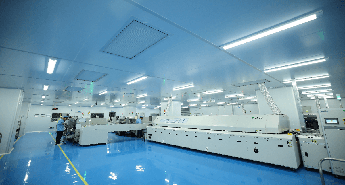
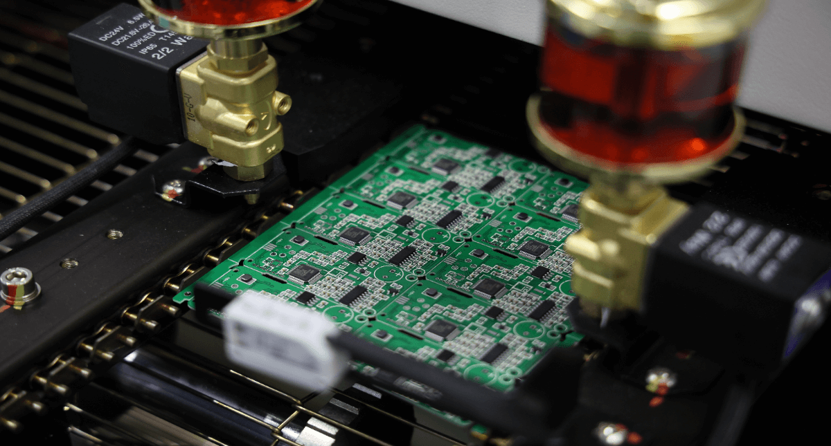
11、Assembly The assembled PCB involves placing components on the finished board and ensuring that all connections are secure. This stage usually requires a combination of automated machinery, precision tools, and manual labour.
12、Final Testing The final stage of the process process involves testing the assembled device to ensure that it is functioning correctly. This test is performed by powering the device and running it through a series of functional tests.
13、Packaging and Shipping The final stage of the process is to package the PCB unit and ship it to its intended location. This stage includes quality control checks for packaging material, documentation, and labelling.
14、Quality Control Throughout the entire PCB manufacturing process, quality control measures are critical to ensuring that the final product meets the desired specifications. Quality control involves inspections throughout the process, ensuring that each stage is completed according to the design specifications and standards.
15、Customer Support and Maintenance Even after the product has been shipped to the customer, customer support is essential to ensure optimal operation of the device. This support includes technical assistance, repair services, and product upgrades as needed.
Conclusion: In conclusion, the manufacturing and assembly of PCBs involves a complex and detailed process that requires careful attention to each stage being completed accurately and efficiently. Understanding the PCB manufacturing process flowchart can help you appreciate the complexity of the process and gain a better understanding of the various stages involved in producing a high-quality PCB. By ensuring that all stages are completed according to established specifications and standards, you can be confident that your PCB will meet your needs and serve its intended purpose effectively.
Comment on this article here
-
No comment

Ripple
Hi everyone, I'm Ripple, Sales Director of KFPCBA Tech Ltd. If you are looking for a one-stop PCB and PCB assembly manufacturer in China, KFPCBA is your best choice! Please feel free to contact our team! Thanks!
Contact me now


