


 tel:+86-18825224069
 email:
 address:201, Factory 6, Longhui Industrial Park, Fuqiao 3rd District, Xinhe Community, Fuhai Street, Baoan District, Shenzhen china
RF Circuit Design Design Is Now Back In The Mainstream
Release date:2022-11-28 14:56:10 Number of views:76
RF circuit design design is now back in the mainstream, designers who are not familiar with RF design
Digital system designers may be familiar with some RF components and layout styles, but there is much more to RF circuit design. RF circuits can include integrated circuits, discrete semiconductors, and printed RF components that work together to produce the desired function. RF circuit design involves combining all of these elements to build the overall system and create the PCB layout.

RF circuits are not as intuitive as typical circuit diagrams, and sometimes diagrams can violate basic electrical design rules. However, due to the propagation properties of electromagnetic fields, circuits operating at RF frequencies behave very differently than typical integrated circuits operating at DC or digital frequency bands. Whether you're designing a wireless communication system or just need to design a transmission line with a specific impedance, be aware of these basics of microwave engineering.
It's often joked that radio frequency (RF) design of integrated circuits and PCBs is all you need to know to pass college qualifications. However, many of today's application-specific products will require the use of mixed-signal components, integrated wireless communication modules, or support for high-frequency applications such as radar. RF design is now back in the mainstream DCBoard Design Designers new to RF design should read this guide to improve their skills.
Introduction to RF Circuit Design
RF circuits are designed to mimic standard circuit elements and some simple integrated circuits by building structures using printed elements on a circuit board. RF circuits may seem a little foreign to DC board design , since they don't always use off-the-shelf components. Instead, RF circuits can provide the required functionality on the board using printed traces on the PCB and some additional components.
Printed RF Circuits
The printed portion of the RF circuit board will use copper traces to build the circuit elements. The arrangement of microstrip lines, capacitor or inductor elements, and semiconductors in an RF circuit may not seem intuitive, but they exploit the behavior of propagation in electromagnetic fields to produce the desired electrical behavior. There are some important conceptual points to remember about RF circuit design, and how an RF circuit on a PCB behaves electrically:
Passivity: All printed RF circuits are passive unless active off-the-shelf components are added to the design. However, research has been conducted on active RF components built entirely from printed traces.
Linear: RF circuits made of printed traces are always linear, meaning that voltage and current are related by a linear function (straight line on the graph). These circuits become nonlinear only when nonlinear semiconductor elements such as diodes are added to the circuit.
Propagation: All radio frequency circuits utilize wave propagation. This means that the input impedance needs to be used when determining how to match the impedance around the circuit and how to create the interface between the different parts of the RF circuit.
Signal Integrity: RF signal integrity relies on electromagnetic shielding and isolation because RF signals need to be as noise-free as possible. Many unique shielding structures and layout techniques have been devised to help provide the required shielding and isolation in RF systems.
Active RF circuit
Active RF circuits can include anything from oscillators to driving amplifiers, ADCs and transceivers. In addition to printed traces, these components can also be used to provide additional functionality. Many radar modules, wireless systems, amplifiers and telecom components will use active components and passive circuits to route RF signals and provide the desired signal propagation behavior. Signal sampling, manipulation, and processing are performed by active components that also provide the interface back to the digital system.
Layout planning
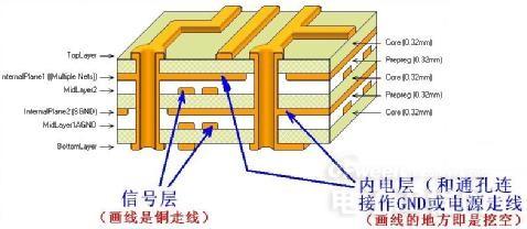
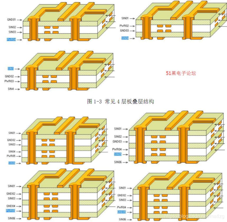
Just like high-speed digital PCBs, successful RF circuit design relies on building a PCB stackup that can support the RF circuit. The stackup should be designed so that the RF components have the desired characteristic impedance, although the impedance of the system will be a more complex function of the RF circuit layout and routing. Also, the relative frequency at which your board will operate will determine how the stackup should be built, what type of printed circuit you may need, and what RF components you can use. RFIC design follows many of the same philosophies as RF PCB design, and mastering these concepts will help you succeed in any area of RF design.
RF circuit board material
FR4 material is suitable for RF transmission lines and interconnects operating at WiFi frequencies (~6 GHz). Beyond these frequencies, RF engineers suggest alternative materials to support RF signal propagation and printed RF circuit designs. Standard FR4 laminates use a resin-filled fiberglass weave to hold components in place, but these fiber weaves in some materials can create signal and power integrity issues if the manufacturing process is not properly specified.
Alternative material systems use PTFE-based laminate and adhesive layer materials to bond the PTFE layer to the next layer in the PCB stackup. These materials have lower loss tangents than FR4 materials, so the signal can travel farther without attenuation and still be within acceptable limits. These laminates should form the substrate to support high frequency radio frequency transmission lines (such as 77 GHz radar) or low frequency very long interconnects (such as 6 GHz WiFi). The table below summarizes some important material properties of common RF PCB materials.
PCB stackup with RF materials
Once you've selected your laminate and bondply materials for your RF design, it's time to add them to your layup. While you can build an entire multilayer PCB stackup out of RF material, it's often not needed and can be prohibitively expensive. One option is to build a hybrid stackup, where the RF laminate is placed on the top layer to support the RF transmission lines and circuitry, and the inner layers are used to support the ground plane, digital signal routing, and power. The opposite layer can also support digital components that need to interface with the RF front-end, any ADCs or other components used to collect RF signals.
If you don't need a digital section in your RF PCB layout, you can use a 2- or 3-layer PCB with standard or near-standard thickness RF laminate. Once the PCB layer thickness and material system are determined, the impedance of the RF traces needs to be determined.
Calculating RF Trace Impedance
After determining the stackup, you need to calculate the width of the conductors on the PCB to produce the desired impedance (typically 50 ohms) in your RF circuit. Some formulas are derived using a technique called conformal mapping to relate the impedance of a trace and its size. Currently, the best resource for finding formulas to calculate trace impedance with complex permittivity is Brian C.'s Transmission Line Design Handbook. However, these formulas cannot solve for a specific width, so a numerical technique is required to determine the width required for a transmission line to have a specific impedance.
For more complex arrangements, such as offset striplines or waveguides, a better option is to use a stack-up design tool with an integrated field solver. These utilities can account for copper roughness, taper during manufacturing, differential routing arrangements, and placement of traces between layers. They are also easy to use in your PCB design software.
Once you know the impedance of the interconnect, you still need to determine the impedance matching requirements by looking at reflection simulation results or looking at the datasheet. For transmission lines used in printed RF circuits, the input impedance of the different transmission line sections is used to determine the impedance match for a given circuit. If you are connecting transmission lines and components in an RF circuit, you need to include the input impedance when designing the RF components and impedance matching network.
Common RF Circuit Designs
It is important to design PCB stackups before designing RF circuits, especially passive RF circuits, as they need to meet specific impedance targets to function properly. In addition, printed RF circuits utilize electromagnetic field propagation on transmission lines, and the propagation behavior will depend on the dielectric function of the substrate material. Once these details are determined, you can start designing your RF circuit and selecting other components for your system.
Printed RF circuits are designed by calculating the portion of the transmission line used for a specific structure on the PCB. Your transmission line design directs propagating waves to components while also providing behaviors such as attenuation, amplification, filtering, resonance, and emission (for example, as an antenna). Impedance transformations are often required at stubs, interfaces to components, and antennas to overcome the impedance mismatch seen by RF signals as they propagate. Various printing structures that yield these functions are well known in many textbooks.
Some of the structures and components used in RF circuits and PCBs include:
Passive and Active Filters
Attenuator
circulator
amplifier
RF Power Dividers, Dividers and Combiners
antenna
resonator
waveguide cavity
After adding the other components, you need to create a schematic of the circuit before you can start the layout. The process for placing an RF circuit in a schematic is the same as it is for a digital system. Circuit simulation is also important in front-end RF engineering because you need to evaluate the electrical functionality of the system before creating the PCB layout. This is typically performed using SPICE simulation in your design, with printed elements in your board defined as transmission line objects in SPICE. The best schematic editors will include transmission line objects to allow you to accurately model electromagnetic behavior in your board.
RF circuit layout tools
Once your RF circuit design is finalized and passed through a circuit simulation tool in your desired frequency range, it's time for the physical layout. RF PCB designers often need to take a mechanical approach to carefully designing their RF interconnects while adhering to standard high-frequency design rules such as minimizing vias and trace length. Any high-frequency circuitry that appears on a PCB needs to be designed to meet impedance targets and geometric tolerances, so your CAD tools need to work in conjunction with your electrical design rules to ensure compliance with these targets.
If you also have digital components that must interface with the RF circuit, you need to use the same toolset to place them in the PCB layout. Careful placement and proper stackup design will help prevent interference with high frequency circuitry and RF signal collection. Native 3D design tools are also helpful here, as some RF systems are multi-board systems that require inspection of the entire assembly before it is ready for fabrication.
When you need to build advanced RF systems while maintaining signal integrity, you need a comprehensive set of circuit simulation tools, PCB routing and layout tools, and layer stack design tools to help you meet your impedance goals. Whether you need to design low-noise amplifiers for signal acquisition, RF power amplifiers for broadcast signals, or complex interconnects with unique trace and via structures, the best PCB layout tools will help you when creating RF Maintain flexibility in PCB layout.
Comment on this article here
-
No comment

Ripple
Hi everyone, I'm Ripple, Sales Director of KFPCBA Tech Ltd. If you are looking for a one-stop PCB and PCB assembly manufacturer in China, KFPCBA is your best choice! Please feel free to contact our team! Thanks!
Contact me now


