


 tel:+86-18825224069
 email:
 address:201, Factory 6, Longhui Industrial Park, Fuqiao 3rd District, Xinhe Community, Fuhai Street, Baoan District, Shenzhen china
Precautions in the design process of 4-layer PCB!
Release date:2022-12-13 16:46:22 Number of views:76
The PCB design process of the four-layer circuit board and related issues that should be paid attention to!
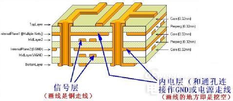
PCB design of four-layer circuit board Author: KFPCBA, anti-interference, embedded system Abstract introduces the PCB design process of the circuit board in detail and the issues that should be paid attention to. In the design process, different layout principles are adopted for ordinary components and some special components; compare the advantages and disadvantages of manual wiring, automatic wiring and interactive wiring; introduce PCB circuits and the measures taken to reduce the interference between circuits related measures. Combined with personal design experience, taking the PCB design of the core board of the embedded system based on ARM and autonomous mobile as an example, briefly introduce the PCB design process of the four-layer circuit board and related issues that should be paid attention to. Printed circuit board (PCB) In electronic products, it plays the role of supporting circuit components and devices, and also provides electrical connections between circuit components and devices. In fact, the design of PCB is not only a 4-layer pcb design for arranging and fixing components , but also the pins of connected devices are so simple, its quality has a great influence on the anti-interference ability of the product. It even plays a decisive role in the performance of future products. With the rapid development of electronic technology, the dimensions of components and products become smaller and smaller, and the operating frequency is higher and higher, which greatly increases the density of components on the PCB, which also increases the difficulty of PCB design and processing. . Therefore, it can be said that PCB design is always one of the most important contents in the development and design of electronic products.
1 、Layout The so-called layout is to reasonably arrange all the components in the circuit diagram on the PCB with limited area. From the signal point of view,

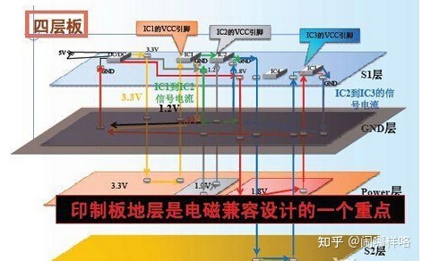
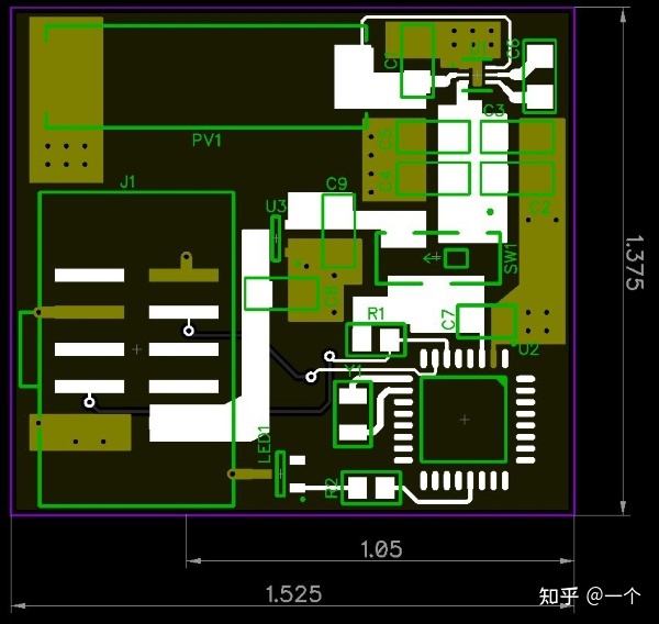
2、there are mainly three types of digital signal circuit boards, analog signal circuit boards and mixed signal circuit boards. When designing a mixed-signal circuit board, careful consideration must be given to placing the components in the proper position on the board by hand in order to separate the digital and analog components, as shown in Figure 1. In the process of arranging the layout of the PCB, the most critical issue is: the 4-layer PCB design such as switches, buttons, knobs and other operating parts and structural parts (referred to as "special components") must be arranged in a designated (suitable) position in advance. After placing, you can set the properties of the components and select the LOCK item, so that you can avoid moving them by mistake in future operations; and for the location arrangement of other components, you must take into account the routing rate and electrical performance of the wiring at the same time. Optimization, as well as the future production process and cost and many other factors. The so-called "combination" is often a challenge to the level and experience of design staff. 1.1 Layout principles of special components
① The connection between components should be shortened as much as possible, and try to reduce their distribution parameters and mutual electromagnetic interference. Components that are susceptible to electromagnetic interference cannot be too close, and input and output components should be as far away from each other as possible.
②There may be a high potential difference between some components or wires, so the distance between them should be increased to avoid accidental short circuit caused by discharge; at the same time, from the perspective of safety, components with high voltage should be as far as possible Arrange it in a place where hands are not easy to reach during debugging.
③For components with a mass exceeding 15g, they should be fixed with brackets before soldering. Those large and heavy components with high heat generation should not be installed on the printed board, but should be installed on the chassis bottom plate of the whole machine...
Comment on this article here
-
No comment

Ripple
Hi everyone, I'm Ripple, Sales Director of KFPCBA Tech Ltd. If you are looking for a one-stop PCB and PCB assembly manufacturer in China, KFPCBA is your best choice! Please feel free to contact our team! Thanks!
Contact me now
Relevant content you may be interested in
Related articles


