


 tel:+86-18825224069
 email:
 address:201, Factory 6, Longhui Industrial Park, Fuqiao 3rd District, Xinhe Community, Fuhai Street, Baoan District, Shenzhen china
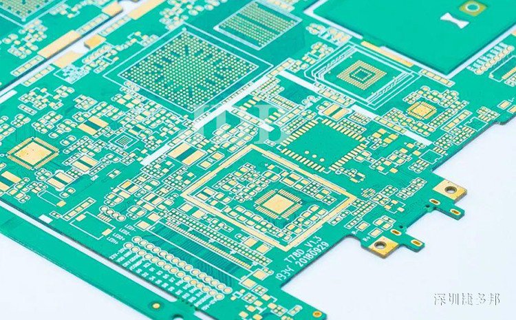
Design Suggestions For Laminated Structure In PCB Design-Shanghai Yijian Medicine
Release date:2022-11-25 18:43:22 Number of views:115
Design Suggestions for Laminated Structure in PCB Design -Shanghai Yijian Medicine
Design suggestions for stacked structures in PCB design:
1. The PCB stacking method is recommended as the Foil stacking method
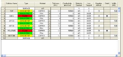
2. Minimize the use of PP sheets and CORE models and types in the same stack (no more than 3 PP stacks per layer of media)
3. The thickness of the PP medium between the two layers should not exceed 21MIL (thick PP medium is difficult to process, generally adding a core board will lead to an increase in the actual number of layers and additional processing costs)
4. The outer layer (Top, layer) of the PCB generally uses 0.5OZ thick copper foil, and the inner layer generally uses 1OZ thick copper foil
Note: Generally, the thickness of the copper foil is determined according to the size of the current and the thickness of the wiring. For example, the power board generally uses 2-3OZ copper foil, and the ordinary signal board generally chooses 1OZ copper foil. In the case of thinner wiring, 1/3QZ copper foil may be used foil to improve the yield rate; at the same time avoid using a core board with inconsistent copper foil thickness on both sides of the inner layer.
5. The distribution of the PCB wiring layer and the plane layer is required to be symmetrical from the center line of the PCB board stacking (including the layer number pcb stacking design , the distance from the center line to the pcb stacking design , the copper thickness of the wiring layer and other parameters)
Note: The PCB stacking method needs to adopt a symmetrical design. The symmetrical design refers to the thickness of the insulating layer, the type of prepreg, the thickness of the copper foil, and the type of graphic distribution (large copper foil layer, circuit layer) as symmetrical as possible relative to the center line of the PCB.
6. The design of line width and dielectric thickness needs to leave sufficient margin to avoid design problems such as SI caused by insufficient margin
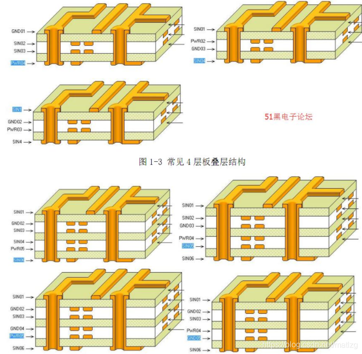
The stackup of PCB consists of power plane, ground plane and signal plane. The signal layer, as the name implies, is the wiring layer of the signal line. The power layer and the ground layer are sometimes collectively referred to as the plane layer.
In a small number of PCB designs, the wiring on the power ground plane layer or the power supply and ground network on the wiring layer are used. This mixed type of layer design is collectively called the signal layer.
The following figure is a typical stacking diagram of 6 layers
Comment on this article here
-
No comment

Ripple
Hi everyone, I'm Ripple, Sales Director of KFPCBA Tech Ltd. If you are looking for a one-stop PCB and PCB assembly manufacturer in China, KFPCBA is your best choice! Please feel free to contact our team! Thanks!
Contact me now


