


 tel:+86-18825224069
 email:
 address:201, Factory 6, Longhui Industrial Park, Fuqiao 3rd District, Xinhe Community, Fuhai Street, Baoan District, Shenzhen china
[Dry Goods] Basic Principles Of High-speed Signal Integrity Design (2)
Release date:2022-11-23 16:14:25 Number of views:147
[Dry goods] Basic principles of high-speed signal integrity design (2)
For the definition of high-speed signals, as mentioned in the previous article, when the clock frequency of the signal exceeds 5MHz, or the signal rise/fall time is less than 5ns, it is generally necessary to use a multi-layer board design. The reason is that the multi-layer board design can effectively control the area of the signal loop to obtain excellent electrical performance.
The stacked structure design of PCB is the basis for signal integrity analysis. The general principles are as follows:
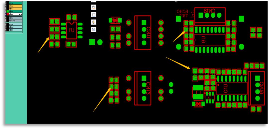
Example 1
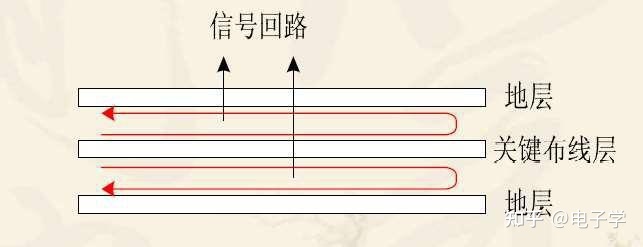
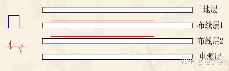
For multi-layer boards, key wiring layers (clock lines, bus lines, interface signal lines, radio frequency lines, reset signal lines, chip select signal lines, and various control signal lines) should be adjacent to the complete ground plane, preferably two ground planes. between planes. The key signal lines are generally strong radiation or extremely sensitive signal lines, and wiring close to the ground plane can reduce the area of the signal loop, thereby reducing its radiation intensity or improving the anti-interference ability.
Example 2
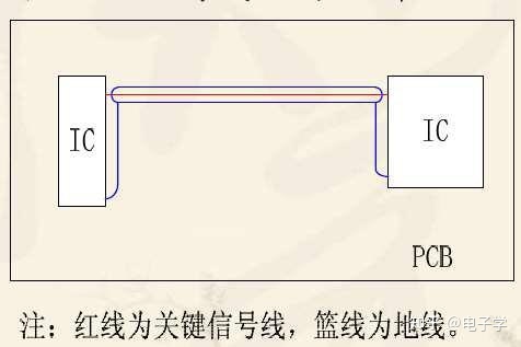
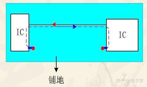
For single-layer boards, "Guide Lines" should be placed on both sides of the key signal line. On the one hand, it can reduce the area of the signal loop, and on the other hand, it can prevent crosstalk between the signal line and other signal lines. The layout method As shown below:
Example 3
If it is a double-layer board, it is required to have a large area of ground on the projection plane of the key signal line. You can also refer to the design method of the single-layer board and use the "defense ground wire".
Example 4
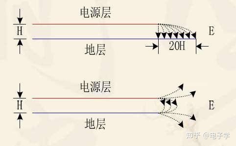
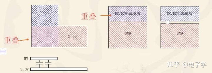
In multi-layer boards, the power plane should be retracted relative to its adjacent ground plane (5~20H is recommended), which can effectively suppress the "edge radiation" problem.
Example 5
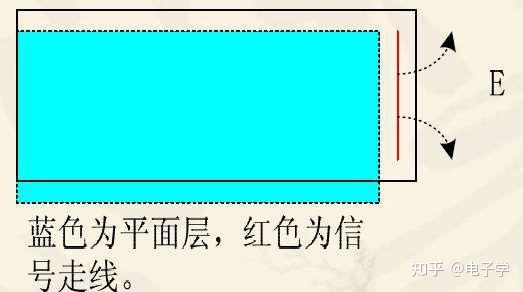
If the wiring layer is not in the projection area of its reflow plane layer, the signal line will be exposed outside the projection area during wiring, which will cause the problem of "edge radiation", and will also increase the loop area of the signal, and at the same time, the differential mode radiation will get bigger. Therefore, the projection plane of the wiring layer should be in the area of its reflow plane layer.
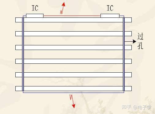
Example 6
When designing multi-layer boards, it is also necessary to pay attention to whether there are no signal lines ≥ 50MHz on the top and bottom layers of the board. It is best to route high-frequency signal lines between the two plane layers to suppress its radiation to space.
Example 7
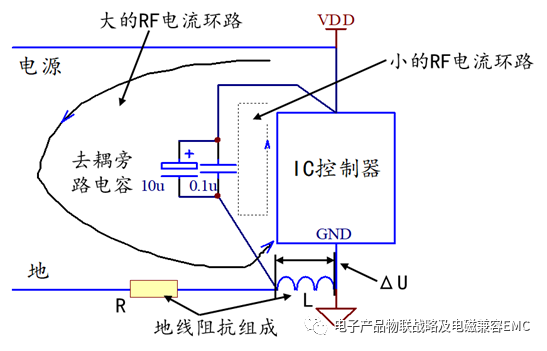
In a multi-layer board, the main working power plane of the board (the most widely used power plane) should be adjacent to its ground plane, which can effectively reduce the loop area of the power supply current.
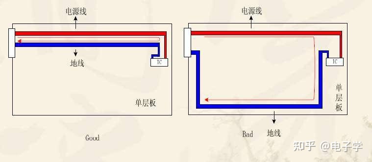
Example 8
In a single-layer board, there must be a ground wire adjacent to the power trace, and the parallel traces are also used to reduce the loop area of the power supply current.
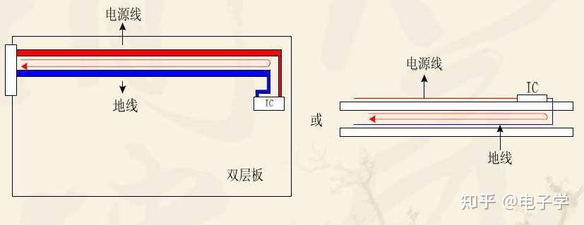
Example 9
In the same way, in a double-layer board, there must be a ground wire adjacent to and parallel to the power trace.
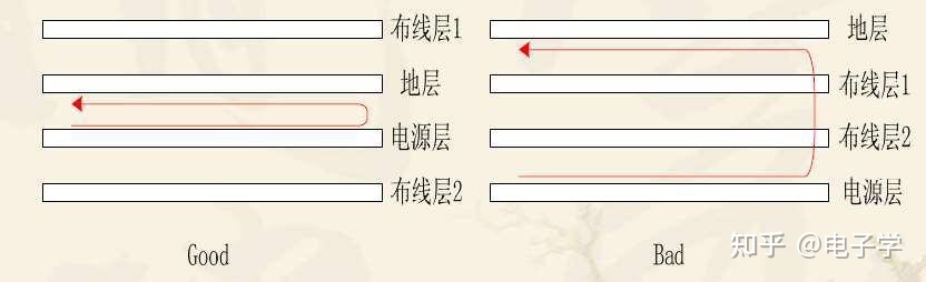
Example 10
In layered design, the design of adjacent wiring layers should be avoided as much as possible. If it cannot be avoided, the layer spacing between the two wiring layers should be appropriately increased, and the layer spacing between the signal layer and its signal loop should be reduced to prevent adjacent wiring layers. Crosstalk caused by parallel signal traces above.
Example 11
Adjacent planar layers should try to avoid overlapping projection planes. When the projection planes overlap, the coupling capacitance between layers will cause noise coupling between layers.
The following will focus on the advantages and disadvantages of the multilayer board stack design scheme. Which scheme to choose should be based on signal quality requirements, manufacturing process requirements, and production costs.
Four-layer board
Solution 1: Signal layer 1 should have more than 8 layers of wiringThe board is designed and contains critical signals so it is directly adjacent to the reference ground plane. The impedance control core board from the ground layer to the power layer should not be too thick to reduce the distributed impedance of the power and ground planes and ensure the decoupling effect of the power plane;
Solution 2: There is no power plane on the whole board, only GND and PGND each occupy a plane, which is suitable for PCB design where most components are plug-ins and the wiring is simple .
Six-layer board
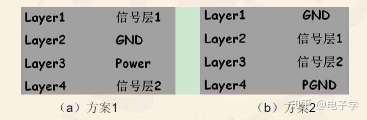
Solution 1: The advantage is that each signal layer has a complete reference layer, and there are no adjacent signal layers, which avoids crosstalk between different signals. The signal layer 2 is the optimal wiring layer, and the power layer and the ground layer are adjacent to the 8-layer circuit board design , so that the power supply impedance is reduced. However, the disadvantage of this solution is also obvious, that is, there are only 3 layers of wiring layers. For the design with a large amount of wiring, we can only choose other solutions or increase the stacking, which will lead to the problem of stacking asymmetry;
Solution 2: The biggest advantage is that the wiring layer reaches 4 layers, and the preferred wiring layers are S1 and S2. The disadvantage is that the ground plane and the power plane are not adjacent, which increases the power supply impedance;
Solution 3: The advantage is that the power supply layer is adjacent to the ground layer, which reduces the power supply impedance, and the wiring layer has reached 4 layers, but S1, S2, S3, and S4 are all exposed, and only S2 has a better reference plane. S1 and S2, S3 and S4 are prone to crosstalk.
Eight-layer board
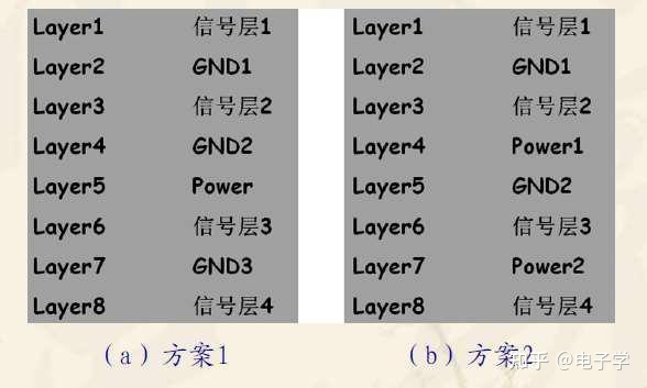
At present, there are many options for stacking design schemes of eight-layer boards in the industry, but scheme 1 and scheme 2 are still recommended, among which scheme 1 is the best choice, which can achieve perfect impedance control;
And option 2 should choose S1 and S2 as the priority wiring layer, and set it as the main power supply at the same time.
Stackup Design Comparison Table
The above are the practical skills of high-speed circuit board stack design. How to apply it to the design of actual products depends on the different requirements of each product, combined with product specifications, design difficulty, project cycle, cost budget, production process and Only by comprehensively evaluating the supplier's manufacturing capabilities and other factors can a reasonable plan be drawn.
Comment on this article here
-
No comment

Ripple
Hi everyone, I'm Ripple, Sales Director of KFPCBA Tech Ltd. If you are looking for a one-stop PCB and PCB assembly manufacturer in China, KFPCBA is your best choice! Please feel free to contact our team! Thanks!
Contact me now


