


 tel:+86-18825224069
 email:
 address:201, Factory 6, Longhui Industrial Park, Fuqiao 3rd District, Xinhe Community, Fuhai Street, Baoan District, Shenzhen china
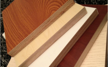
Basic Knowledge of Pcb Single layer Slab Design
Release date:2022-12-15 16:24:00 Number of views:86
pcb single-layer board design the basics related to PCB, to help you give pointers, please look down
The answer is helpful and has reference value
Today, I will give you a popular science about the basics of PCB, and help you to give advice. Please read on.
1. Single panel (-Sided)
We just mentioned that on the most basic PCB, parts are concentrated on one side and wires are concentrated on the other side. Because wire only appears on one side, so we just claim that this PCB is called single-sided board (-sided). Because the single-sided board has many strict restrictions on the design of the circuit (because there is only one side of the pcb single-layer board design , the wiring cannot cross but must go around a separate path), so only the early circuit
Only use this type of board.
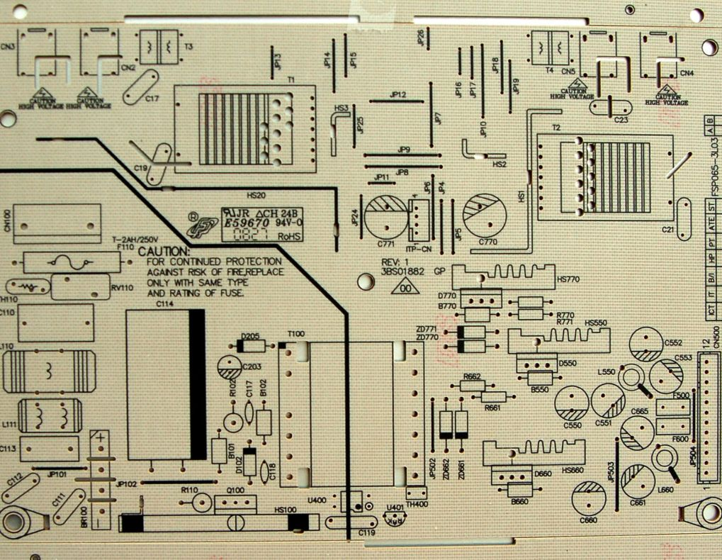
2. Double panel (-Sided)
This type of board has wiring on both sides. However, to use the wires on both sides, there must be a proper circuit connection between the two sides.
This "bridge" between circuits is called a via. The guide hole is a small hole filled or coated with metal on the PCB, which can be connected to the wires on both sides. Because the area of the double-sided panel is twice as large as that of the single-sided panel, and because the wiring can be interlaced with each other (can go around to the other side), it is more suitable for use in circuits that are more complex than the single-sided panel.
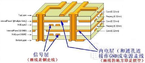
Three, multi-layer board (Multi-Layer)
In order to increase the area that can be wired, more single or double-sided wiring boards are used in multilayer boards. The multi-layer board uses several double-sided boards, and puts a layer of insulating layer between each layer of boards and sticks them firmly (pressing). The number of layers of the board means that there are several independent wiring layers, usually the number of layers is even, and includes the outermost two layers. Most motherboards have a structure of 4 to 8 layers, but it is technically possible to achieve a PCB board with nearly 100 layers. Most of the large supercomputers use fairly multilayer motherboards, but because such computers can already be replaced by clusters of many ordinary computers, super multilayer boards have gradually been out of use. Because the layers in a PCB are so tightly bonded, it's usually not easy to see the actual number, but you might be able to if you look closely at the motherboard.
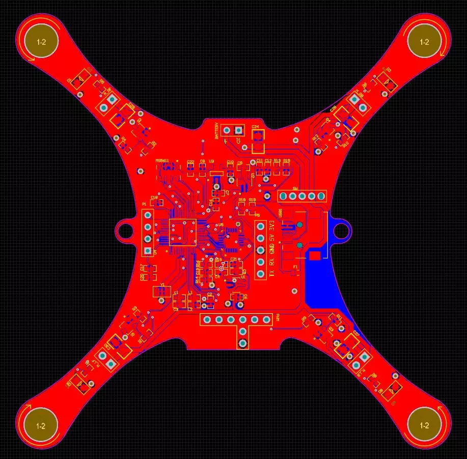
The guide hole (via) we just mentioned, if it is applied on a double-sided board, must penetrate the entire board. However, in a multi-layer board, if you only want to connect some of the lines, then the via
Some line space of other layers may be wasted. Buried hole (vias) and blind hole (Blind vias) technology can avoid this problem because they only penetrate a few layers . Blind hole is how many
The internal PCB of the layer is connected to the surface PCB without penetrating the entire board. The buried hole is only connected to the internal PCB, so it cannot be seen from the surface.
In a multilayer PCB, the entire layer is directly connected to ground and power. So we classify each layer as signal layer (), power layer (Power) or ground layer (). If the parts on the PCB require different power supplies, usually this type of PCB will have more than two layers of power and wire layers.
Comment on this article here
-
No comment

Ripple
Hi everyone, I'm Ripple, Sales Director of KFPCBA Tech Ltd. If you are looking for a one-stop PCB and PCB assembly manufacturer in China, KFPCBA is your best choice! Please feel free to contact our team! Thanks!
Contact me now
Relevant content you may be interested in
Related articles


