


 tel:+86-18825224069
 email:
 address:201, Factory 6, Longhui Industrial Park, Fuqiao 3rd District, Xinhe Community, Fuhai Street, Baoan District, Shenzhen china
Multi-layer Circuit Board Design In DXP At The Entry Level
Release date:2022-12-07 15:34:39 Number of views:51
SO MCU Development Guide 14 This article only introduces the entry-level introduction to multi-layer in DXPCircuit Board Design Methods
SO MCU Development Guide 14
This article only introduces the method of multilayer circuit board design in PCB drawings in DXP at the entry level.
First, the purpose
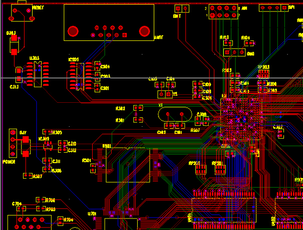
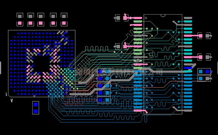
In fact, two layers of a general circuit board are enough, the front and the back, and the wiring can be on one or both sides. However, in complex circuits and high-speed PCB design , sometimes it is necessary to use multiple layers. This means that in addition to the front and back of the circuit board, there are other layers between them, such as internal electrical layers and intermediate layers. This involves To multilayer circuit board design, then this article briefly introduces the method of multilayer circuit board design.
Inner electrical layer (plane): It is a complete plane, the entire copper clad, is a negative corrosion, that is, the place where the wiring is corroded, can be used as a power layer and a ground layer.
Intermediate layer (layer): It is the same as the ordinary signal layer, positive corrosion, that is, where there are traces, copper is poured, which can be used as traces.
2. Main content
This article introduces the operation steps of creating multiple layers in the PCB drawing in DXP, as well as some necessary setting methods.
Three, multi-layer circuit board design
3.1 What is a multilayer circuit board
A multilayer circuit board has at least three conductive layers, two of which are on the outer surface, while the remaining layer is synthesized inside the insulating board.
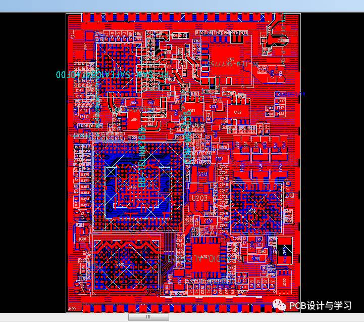
In the production process, after making each layer of circuit, it is positioned and pressed by optical equipment, so that the multi-layer circuit is superimposed on a circuit board, which is called a multi-layer circuit board.
3.2 How to wire between layers
The electrical connection between them is usually achieved through plated through holes on the cross-section of the circuit board, that is, vias.
3.3 Building a multi-tiered approach
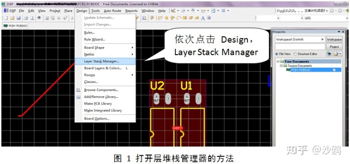
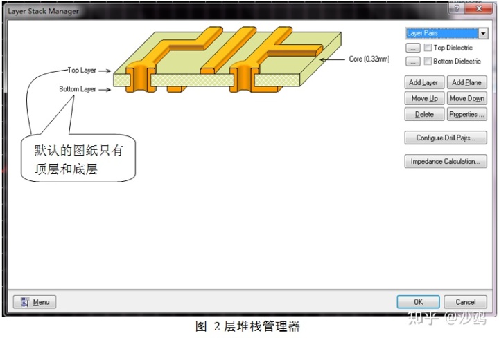
When creating a new PCB drawing in DXP, there are only two layers, the front and the back, by default. To create a new layer between the front and the back of the PCB, you need to design the pcb multilayer circuit board in the "layer stack manager" . The operation steps are as follows:
1. Open the layer stack manager
Click on the menu bar of the PCB drawing interface: →Layer Stack to open the layer stack manager.
2. The method of increasing the signal layer (intermediate layer)
(1) First select any layer, such as layer or top layer;
(2) Click the add layer button again to add a signal layer;
(3) After adding, click OK to complete the operation.
3. The method of increasing the internal electric layer
(1) First select any layer, such as layer or top layer;
(2) Click the add plane button again to add an internal electrical layer;
(3) After adding, click OK to complete the operation.
3.4 Layer Settings
After creating a new layer, it may not be visible in the layer management bar at the bottom of the PCB drawing. What's the matter?
One reason is not shown. Here's how to make it show up:
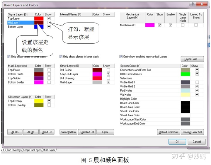
(1) In the PCB drawing interface, press the shortcut key L to open the "Layer and Color Panel",
(2) Tick the show of the corresponding layer, and the corresponding layer can be displayed in the layer management column at the bottom of the PCB drawing.
Four. Summary
This article only briefly describes the method of creating and setting the middle layer of the circuit board. It is definitely not finished, and the specific wiring and other content will be updated later.
Comment on this article here
-
No comment

Ripple
Hi everyone, I'm Ripple, Sales Director of KFPCBA Tech Ltd. If you are looking for a one-stop PCB and PCB assembly manufacturer in China, KFPCBA is your best choice! Please feel free to contact our team! Thanks!
Contact me now
Related articles


