


 tel:+86-18825224069
 email:
 address:201, Factory 6, Longhui Industrial Park, Fuqiao 3rd District, Xinhe Community, Fuhai Street, Baoan District, Shenzhen china
Eight-layer PCB board production process
Release date:2023-02-24 17:44:56 Number of views:75
The production process and detailed introduction of the eight-layer board (with detailed process)
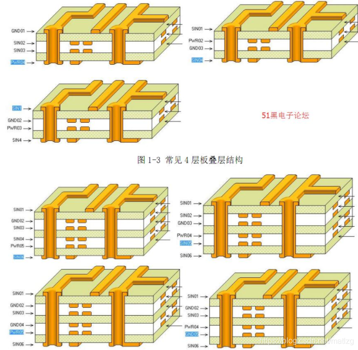
Three stacking methods of PCB eight shelves
Eight shelves generally use the following three stacked forms:

The first:
The first layer: device surface, microstrip wiring layer
The second layer: internal microstrip routing layer, better routing layer
Layer 3: Bedrock
The fourth layer: stripline wiring layer, better wiring layer
The fifth layer: stripline wiring layer
The sixth layer: power layer
Seventh layer: internal microstrip routing layer
Eighth layer: microstrip routing layer
It can be understood from the above description that such a stacking method has only one power supply layer and one bedrock, so the electromagnetic absorption capacity is relatively poor and the power supply impedance is relatively large, which makes this form not a good stacking method.
The second type:
The first layer: device surface, microstrip wiring layer 8-layer PCB design , good wiring layer
The second layer: rock mass, better electromagnetic wave absorption capacity
The third layer: stripline wiring layer, good wiring layer
The fourth layer: the power layer, which forms excellent electromagnetic absorption with the bedrock below
Fifth Layer: Bedrock
The sixth layer: stripline wiring layer, good wiring layer
The seventh layer: rock mass, with large power impedance
The eighth layer: microstrip wiring layer, good wiring layer
It can be seen from the previous description that these methods reduce the reference layer, have better EMI performance, and the characteristic impedance of each signal layer can be well controlled.
The third type:
The first layer: device surface, microstrip wiring layer, good wiring layer
The second layer: rock mass, better electromagnetic wave absorption capacity
The third layer: stripline wiring layer, good wiring layer
The fourth layer: the power layer, which forms excellent electromagnetic absorption with the bedrock below
Fifth Layer: Bedrock
The sixth layer: stripline wiring layer, good wiring layer
The seventh layer: rock mass, better electromagnetic wave absorption capacity
The eighth layer: microstrip wiring layer, good wiring layer
The third stacking method is the best stacking method 8-layer PCB design , because these methods use multiple layers of ground reference planes, which have particularly good geomagnetic absorption capabilities.
Let's explain the stackup and impedance from a previous project.
As shown in the picture above, this project is made of 8 shelves, and 3 core boards are used for lamination (both sides contain copper plates, which can be regarded as a two-shelf board), and 3 core boards have 6 boards. 8 layers, and the prepreg and copper plates are stacked on both sides to form an 8-shelf.
Trace impedance design requirements:
1. The highlighted part of the L8 layer refers to L7 to make an impedance of 100 ohms
2. The highlighted part of the L3 layer refers to L2/L4 to make an impedance of 100 ohms
3. The highlighted part of the L8 layer refers to L7 to make an impedance of 90 ohms
4. The highlighted part of the L8 layer refers to L7 to make an impedance of 50 ohms
5. The highlighted part of the L6 layer refers to L5/L7 to make an impedance of 50 ohms
6. The highlighted part of the L3 layer refers to L2/L4 to make an impedance of 50 ohms
7. The highlighted part of the L1 layer refers to L2 to make an impedance of 50 ohms
KFPCBA is a circuit board manufacturer of high-precision multi-layer PCB industrial-grade products, with 20 years of rich experience in board making, and ingenuity to make good boards!
PCB board making , PCB design , BOM distribution list, FPC flexible board, SMT placement one-stop service provider!
You can find us by searching "KFPCBA" or "KFPCBA".
Comment on this article here
-
No comment

Ripple
Hi everyone, I'm Ripple, Sales Director of KFPCBA Tech Ltd. If you are looking for a one-stop PCB and PCB assembly manufacturer in China, KFPCBA is your best choice! Please feel free to contact our team! Thanks!
Contact me now
Relevant content you may be interested in
Related articles


