 address:201, Factory 6, Longhui Industrial Park, Fuqiao 3rd District, Xinhe Community, Fuhai Street, Baoan District, Shenzhen china
[Knowledge Points] Electrical Rules Based On Circuit Board Wiring (1)
[Knowledge points] Electrical rules based on circuit board wiring (1)
1. Electrical rules (rules)
The electrical design rules are used to set the electrical rules followed in the circuit board wiring process, including the four rules of safety spacing, short circuit, unrouted network and unconnected pins:
(1), safe distance rules ()
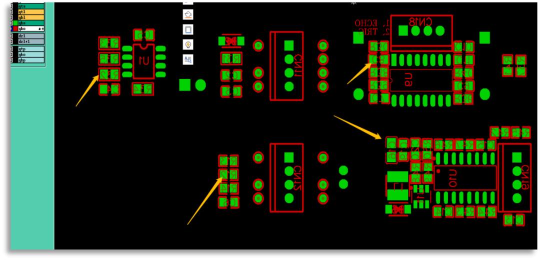
This rule is used to set the safe distance between objects such as wires, vias, pads, and copper fills in PCB design .
The rules of the safety distance are expanded in a tree structure. Click a rule name in the safety distance rule tree with the mouse, for example, the right area of the dialog box will display the range used by this rule and the constraint characteristics of the rule --- For example, the rules restrict the safe distance between the polygonal copper pour in the PCB file and other objects in the file, such as traces, pads, vias, etc., to be 0.5mm.
(2), short-circuit rule (short-)
This rule sets whether the wires on the circuit board are allowed to be short-circuited. If the allow short check box is selected in the area of the constraint dialog box of this rule, the short-circuit is allowed, otherwise the short-circuit is not allowed. ---Generally keep the default
(3), unwired network rules (net)
This rule is used to check whether the network within the specified range is successfully routed. If there is an unsuccessful route in the network, the wires that have been routed on the network will be retained, and the wires that have not been successfully routed will remain flying wires. ---Generally keep the default
(4), unconnected pin rule ()
This rule is used to check whether the component pins within the specified range are connected successfully. The default is an empty rule, if you need to design related rules, you can add them.
2. Wiring rules (rules)
Wiring rules are mainly rules related to wiring settings, and there are the following seven categories:
(1), wiring width (width)
This rule is used to set the wiring width during wiring. Users can set trace widths for dictation-specific nets, such as power nets. Generally, each specific net routing width rule needs to add a rule in order to distinguish other nets.
There are three width constraints in the pink box in the area, namely: minimum width, preferred width and maximum width (respectively described in order from left to right). There are also four options in this area, namely: check the minimum/maximum width of the wire/arc respectively, check the minimum/maximum width of the copper connection, the line width driven by the characteristic impedance, and only for the layers in the layer set Wiring layers (indicated sequentially from top to bottom respectively).
(2), wiring method ( )
This rule is used to define the routing between pins.
There are seven wiring methods in this rule, and the order from top to bottom indicates that the wiring methods are: wiring by the shortest path, wiring mainly in the horizontal direction (horizontal to vertical ratio is 5:1),
Wiring method mainly in vertical direction (vertical and horizontal ratio is 5:1), simple chrysanthemum wiring method (you need to specify the start point and end point, otherwise it is the same as the method), middle-driven chrysanthemum-like wiring method (you need to specify the start point and end point , otherwise the same as the method), balanced chrysanthemum wiring (need to specify the starting point and end point, otherwise the same as the method), radial wiring. ---Need to be set during automatic routing
(3), wiring priority level ( )
This rule is used to set the priority of routing, and the network or object with higher priority will be routed first. The priority level can be set from 0 to 100, and the higher the number, the higher the priority level. You can directly enter the number setting in the option or use the increase and decrease buttons on the right to adjust it. ---Need to be set during automatic routing
(4), wiring board layer ( )
This rule is used to set the board layers that allow automatic routing. By default, the top layer is vertical and the bottom layer is horizontal (if you want to change the routing direction, you can execute auto route-->set up, and then click the situs dialog box edit layer button, open the layer routing direction setting dialog box to set the routing direction). ---Need to be set during automatic routing
(5), wiring corner ( )
This rule is used to set the corner mode of automatic routing. There are three routing modes: 45°, 90° and arc corner. ---Need to be set during automatic routing
(6), wiring via type (via style)
This rule is used to set the via hole size parameters that are automatically placed during the routing process, and set the via hole diameter (via ) and the drilling diameter of the via hole (via hole size) in the area. ---It needs to be set during automatic routing. At the same time, the size of the via hole added when pressing the * key to switch the wiring layer during manual routing is also subject to this rule.
(7), fan-out wiring control ( )
This rule is mainly used for wiring control of special devices such as ball grid array pcb stack design and leadless chip holder. By default, the following five types of fan-out routing rules are included: (ball grid array package fan-out routing), (leadless chip package fan-out routing), (small outline package), (component pins less than five A small package), (system default fan-out routing).
The setting methods of the above five types of fan-out routing rule options are the same, all in the area:
style: fan-out type, used to select the placement relationship between fan-out vias and SMT components. There are auto (fan-out vias are automatically placed in the best position), rows (fan-out vias are placed in two straight lines), rows (fan-out vias are placed in two intersecting rows), BGA (fan-out heavy Now BGA), under pads (fan-out vias are placed directly under the pads of SMT components) to choose from.
: Fan-out direction, used to determine the direction of fan-out. Yes (do not fan out), in only (fan out inward), out only (want to fan out crookedly), in then out (fan out inward first, then fan out outward when there is not enough space), out then in (first There are 6 options: fan out outward, and fan out inward when there is insufficient space), in and out (inside and then outside alternately when fanning out).
from pad: Pad fan-out direction option. There are away from (fan out at 45° to the surrounding), north-east (fan out at 45° to the north), south-east (fan out at 45° to the southeast), north-west (fan out at 45° to the southwest ), north-west (fan out at 45° to the northwest), (fan out to the center) these 6 options.
Via mode: Fan-out via placement mode. There are close to pad (rules) --- close to the pad and pads --- two options between the two pads. ---Need to be set during automatic routing
3. SMT rules (SMT rules)
The SMT rules are mainly aimed at the wiring rules of surface mount components, and there are three types:
(1), surface mount pad lead length (SMD to )
This rule is used to set the minimum distance between the SMD component pad and the corner of the wire. This distance determines how close it is to the pads adjacent to that pad. By default this is an empty rule, you can add new rules as needed.
(2), the connection distance between the surface mount pad and the inner layer (SMD to plane)
This rule is used to set the distance between the SMD and the pad or via of the inner plane. The connection between the surface mount pad and the internal electrical layer can only be realized by vias. This rule setting indicates how far from the center of the SMD pad to use vias to connect to the inner layer. By default this is an empty rule, you can add new rules as needed.
(3), SMD neck down
This rule is used to set the ratio relationship between the width of the wire drawn from the SMD pad and the pad width of the SMD component (the default value is 50%). By default this is an empty rule, you can add new rules as needed.
4. Mask rules
The solder mask/flux coverage rules are used to set the spacing rules of the solder mask layer, solder paste protective layer and pad, and there are two types in total:
(1), solder mask extension ( mask )
Usually, the entire surface of the solder resist layer is covered with solder resist except for pads or vias. The role of the solder mask is to prevent parts that should not be soldered from being connected by tin. Reflow soldering is achieved by solder mask. Another role of the solder mask is to improve the insulation of the wiring, anti-oxidation and aesthetics.
When making a circuit board, first use the solder mask data designed by the PCB design software to make a silk board, and then use the silk board to print the solder resist (solder resist paint) on the circuit board. When the solder resist is printed on the circuit board, the pcb stack design , the pad or via is vacated, if the input is a positive value, the area vacated by the pad or via is larger than the pad or via , if it is a negative value, you can cover the via hole with oil (generally set the value to -1.5mm).
(2), solder paste protective layer expansion (paste mask)
Before soldering surface mount components, first apply a layer of solder paste to the pad, then stick the components on the pad, and then solder with a reflow soldering machine. Usually in mass production, the pasting of surface mount pads is done through a steel mold. The position corresponding to the pad on the steel mold is hollowed out according to the shape of the pad. When applying paste, first cover the steel mold on the circuit board, then put the solder paste on the steel mold, and use the bracket to expand back and forth, and the solder paste will pass through the hollow. The part is coated on the pad.
The data of the solder paste layer or solder paste protection layer of the PCB design software is used to make the steel mold. The area of the hollowed out steel mold is smaller than the area of the design pad. The rule is to set the maximum value of this difference (that is, the steel mold) The difference between the hollow area on the mold and the area of the design pad, the default value is 0).
5. Plane rules
The internal electrical layer rules are used to set the wiring of the power supply layer and copper clad layer (P, G), mainly for the connection method and safety distance between the power supply layer and copper clad layer and objects such as pads, vias or wiring. There are three categories:
(1) Connection type of power plane (power plane style)
This rule is used to set the connection type of via or pad to the power plane. There are three connection types to choose from: gap connection, direct connection and no connection; (the number of wires) indicates the number of connection lines between the pad and the internal electrical layer or copper clad layer when gap connection ( ) is selected, and there are two wires or four lines; width is used to set the width of the connection line; air-gap is used to set the gap width when the gap is connected; it is used to set the distance from the center line of the pad or via hole to the inside of the gap. ---Available for four-layer boards or boards with more than four layers
(2), power layer safety distance (power plane)
This rule is used to set the safety distance between the power board layer and the pad or common space passing through this layer (the distance between the inner wall of the pad or via hole and the copper sheet of the power layer). ---Available for four-layer boards or boards with more than four layers
(3), copper clad connection method (style)
This rule is used to set the connection method between copper pour and pads, vias and traces. In the area, the settings of style and width are the same as those of the connection type of the power layer, and the connection angles are 45° and 91°.
6. Test point rules (rules)
Test point rules are used to style and use test points. There are two types of bare board test points and assembly test points, which are generally not used in the design, so they will not be introduced.
7. Manufacturing rules (rules)
Manufacturing rules are mainly set in the content related to circuit board manufacturing. There are nine categories:
(1), minimum ring width (ring)
This rule is used to set the minimum ring width, which is the difference in radius between a pad or via and its drilled hole.
(2), the minimum angle (acute angle)
This rule is used to set the minimum angle between wirings with electrical characteristics, and the minimum angle should not be less than 90°, otherwise it is easy to leave drugs after etching, resulting in over-etching.
(3) Drilling size (hole size)
This rule is used to set the size of the drill diameter of the pad or via.
(4), drilling layer pairs (layer pairs)
This rule is used to set whether drilling ply pairs are allowed.
(5), safe distance between drilling and drilling (hole to hole)
This rule is used to set the safe spacing between boreholes (the distance between the inner wall of the borehole and the inner wall of the borehole). When allow micro vias is checked, it means that micro vias are allowed to stack.
(6), the minimum solder resistance ( mask )
This rule is used to set the width of the minimum solder mask, the default is 10mil.
(7), silk screen on exposed component pads (over pads)
This rule is used to set the safe distance between the component pad and the silk screen.
(8), the text is marked on the safety distance between any components (silk to silk)
This rule is used to set the safe distance between the text label and any component, such as the safe distance between the silk screen and the silk screen.
(9), flying lead tolerance (net)
-
No comment


 tel:+86-18825224069
 email:


