


 tel:+86-18825224069
 email:
 address:201, Factory 6, Longhui Industrial Park, Fuqiao 3rd District, Xinhe Community, Fuhai Street, Baoan District, Shenzhen china
printed circuit board PCB routing and layout planning method
Release date:2022-12-09 16:57:28 Number of views:77

The planning layout and layout method of self-provided wires for PCB wiring of printed circuit boards !
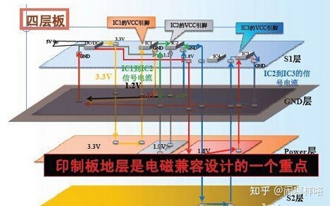
1. Four-layer PCB drawing program:
1. Draw a schematic diagram of the circuit and make a netlist.
The process of drawing the schematic diagram involves the drawing of the elements and the drawing of the package. There is no problem in mastering these two drawing schematic diagrams. Troubleshooting errors and warnings can solve common problems. Complex diagrams can be drawn using hierarchical diagrams.
Shortcuts used here: Ctrl+G (set mesh spacing), CTRL+M (measure the distance between two points)
2. Design the board.
How many layers of planks are used? Do you use single-sided elements or double-sided? What is the size of the board? Wait a moment
3. Set parameters.
Layout parameters. Layer parameters. Basically according to the system preset values, only a small number of parameters are set.
picture
4. Loading of web forms and component packages.
Design -> Update..
Note: If there is an error in the multilayer pcb design when drawing the schematic diagram , but the layout of the PCB has been designed, and it is hoped that the error can be corrected without affecting the PCB layout, then this step must be performed, only in the previous Add do not tick Choose!!! Otherwise, it will be revised, which is really painful!!
The network form is the interface between the circuit schematic diagram editing software and the printed circuit board PCB design software. Only after the circuit board is loaded, the circuit board can be automatically routed.
5. Layout of components.
Most are manual layouts, or a combination of automatic and manual.
If you want to place the component on both sides: select the device and press the left mouse button, and then press the L key; or click the component on the PCB interface, and modify its property as .
Notice:
Parts are discharged evenly, which is convenient for installation, plug-in and welding operations. The typesetting level of the words, the reasonable position, the direction, avoid being blocked, and easy to make.
6. Wiring
Self-prepared wires: manual wiring (the layout must be planned before wiring, and the internal electrical layer must be coordinated. When passing through the internal electrical layer , the system automatically connects it to the copper film . The connection method and safety distance between mesh copper sheets and non-mesh pads/vias and the inner electrical layer can be set according to regulations.
Comment on this article here
-
No comment

Ripple
Hi everyone, I'm Ripple, Sales Director of KFPCBA Tech Ltd. If you are looking for a one-stop PCB and PCB assembly manufacturer in China, KFPCBA is your best choice! Please feel free to contact our team! Thanks!
Contact me now
Relevant content you may be interested in
Related articles


