


 tel:+86-18825224069
 email:
 address:201, Factory 6, Longhui Industrial Park, Fuqiao 3rd District, Xinhe Community, Fuhai Street, Baoan District, Shenzhen china
Difficulties in Multilayer Circuit Board Calibration
Release date:2022-12-13 16:50:40 Number of views:134
The editor will talk about the difficulties of multi-layer circuit board proofing in detail
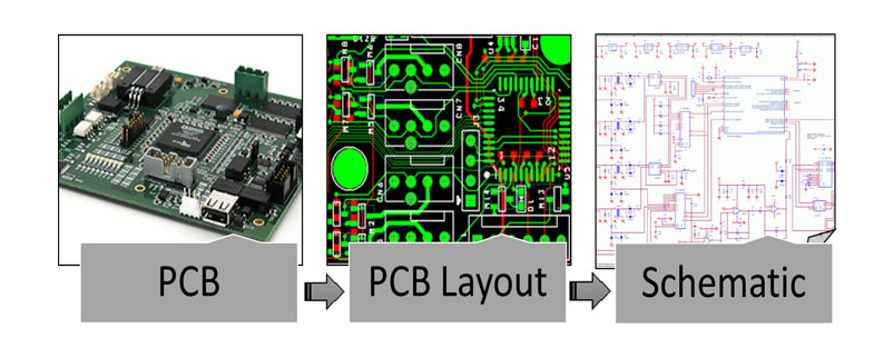
With the continuous development of the electronics industry, pcb has changed from the earliest single-sided board to the current double-sided multi-layer board. Expanded to more than two layers, so multi-layer PCB circuit boards appeared. The following editor will talk about the difficulties of multi-layer circuit board proofing in detail.
1. Difficulties in making internal circuits
Multi-layer circuit boards use special materials such as high TG, high speed, high frequency, thick copper, and thin dielectric layers, which put forward high requirements for internal circuit production and graphic size control. For example, the integrity of impedance signal transmission increases the difficulty of internal circuit fabrication.
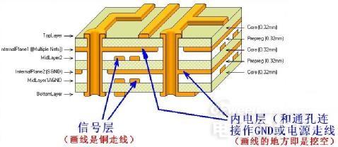
The width and line spacing are small, the open circuit and short circuit increase, the short circuit increases, and the pass rate is low; there are many thin line signal layers, and the AOI leakage detection probability of the inner layer increases; the inner core board is thin, easy to wrinkle, poor exposure, and easy to curl when etching the machine; High-level plates are mostly system boards with large unit sizes and high product scrap costs.
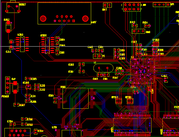
2. Difficulties in interlayer alignment
Due to the large number of layers in the multilayer PCB design , users have higher and higher requirements for the calibration of PCB layers. Typically, the alignment tolerance between layers is controlled at 75 microns. Considering the large unit size of the multilayer circuit board, the high temperature and humidity in the graphic conversion workshop, the dislocation overlap caused by the inconsistency of different core boards, and the positioning method between layers, etc., the centering control of the multilayer circuit board is more difficult.
3. Difficulties in compression manufacturing
Many inner core boards and prepregs are stacked multi-layer PCB designs , which are prone to defects such as slippage, delamination, resin voids, and air bubbles in stamping production. In the design of the laminated structure, the heat resistance, pressure resistance, glue content and dielectric thickness of the material should be fully considered, and a reasonable multilayer circuit board material pressing scheme should be formulated.
Due to the large number of layers, the expansion and shrinkage control and size factor compensation cannot be kept consistent, and the thin interlayer insulation layer is likely to cause the failure of the interlayer reliability test.
4. Difficulties in drilling
The use of high TG, high speed, high frequency, and thick copper special plates increases the difficulty of drilling roughness, drilling burrs and drilling dirt. The number of layers is large, the cumulative total copper thickness and plate thickness are easy to break when drilling; there are many dense BGAs, and the CAF failure problem is caused by narrow hole wall spacing; the problem of inclined drilling is easily caused by the thickness of the plate.
The above is: Xiaobian sorted out the difficulties of multi-layer PCB circuit board proofing, I hope it will be helpful to everyone, if there are still unclear points, please contact our customer service to answer you.
Comment on this article here
-
No comment

Ripple
Hi everyone, I'm Ripple, Sales Director of KFPCBA Tech Ltd. If you are looking for a one-stop PCB and PCB assembly manufacturer in China, KFPCBA is your best choice! Please feel free to contact our team! Thanks!
Contact me now


