


 tel:+86-18825224069
 email:
 address:201, Factory 6, Longhui Industrial Park, Fuqiao 3rd District, Xinhe Community, Fuhai Street, Baoan District, Shenzhen china
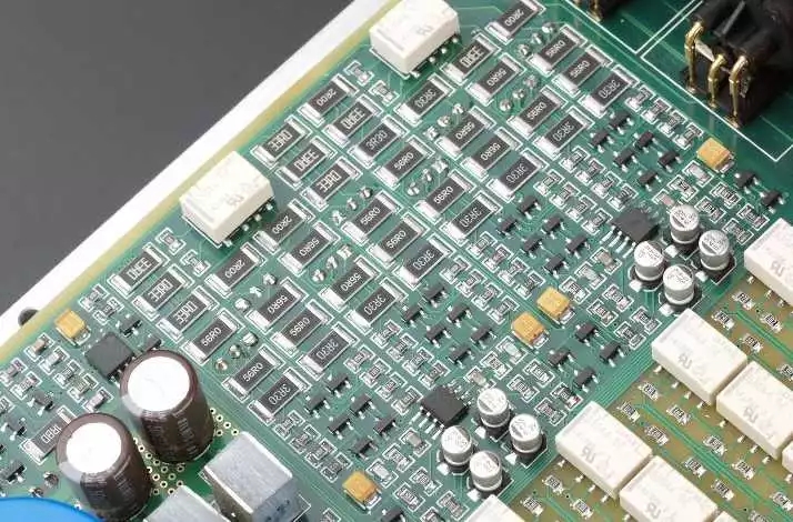
First Steps In A Multilayer PCB Design Tutorial
Release date:2022-12-06 16:16:23 Number of views:130
First steps in a multilayer PCB design tutorial; setup and preparation in some cases
First Steps in the Multilayer PCB Design Tutorial; Setup and Preparation
In some cases, older legacy PCB footprints may not be sufficient for multi-layer designs, so you will need to determine if there are any additional requirements. Depending on the CAD system used, you may have to add layers or attributes to the schematic for multilayer use. Having access to more advanced PCB design systems here with links to online library services would be a real bonus. Using the latest and most accurate PCB footprint source data can be a lot easier.
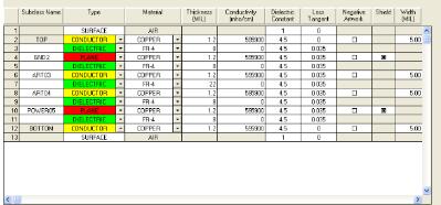
The main difference between a two-layer and multilayer board setup is planning your layer stackup. Here are some key points to consider when planning your board layer stack-up:
· Performance: how fast the circuit will run pcb multilayer circuit board design , and the operating environment of the final circuit board, may affect the material from which the circuit board is made. There are various materials higher than FR-4 that may be better suited for your application depending on your needs, but these may affect parameters such as impedance calculations. Here, the help of your PCB manufacturer will be a valuable source of information.
Cost: The materials of manufacture as well as the number of layers and configuration will directly affect the overall cost of building the board. Here again, you need to consider all options with the manufacturer.
Density: The wiring density of the board is another factor in determining the layer stack configuration of the board. It's a pain when you have to go back and add layers to your board design after you've already started layout. Not only will you need to reconfigure the CAD database, but you may also have to make a lot of changes to the layout. On the other hand, if you're starting with too many layers, then you'll be paying more for the board, then you should.
Circuitry: You also need to understand the needs of the circuit in order to create the best layer configuration. Such as pcb multi-layer circuit board design , in order to obtain the best performance, sensitive signals may need a stripline layer configuration, which means adding other ground planes. The analog and digital circuit areas will need to be separated with their own ground planes, and the on-board power supplies will need to be isolated. All of these can affect layer configuration, so this should be planned before layout begins.
Once the data has been collected and the layer stack created in the layout database, board placement and routing can begin.
Using a tool like this board outline generator makes it easier to create board layer stacks
Different perspectives on location and route
One of the first things that differentiates you when working on a multi-layer layout is that you need to start thinking about the "3D" design aspect. Two-layer boards only require you to think about "top" and "bottom". Now you're in a multi-layered world with a lot of different things going on inside that can affect the top and the bottom. For example, you might not want to place a noisy part somewhere due to sensitive routing on the inner layers beneath it.
As far as tooling is concerned, the way components are placed will be the same as on a double-sided board, but the skins used will be different. For example, you don't have to worry about leaving enough space between parts to route since most of them will be routed on internal layers. For sensitive circuits, it is still necessary to use short direct paths on the surface layer, but in most cases you can now use more space. This is also a good thing, because multilayer boards may require more components to be placed.
Internal trace routing and power planes will be interesting, but in the meantime, here are some important considerations:
·
Multi-layer boards will generally have more components and therefore more wiring than double-sided boards, so plan ahead. Depending on the technology of the board, some of these traces may have specific trace width and space or other requirements, such as differential pairs or impedance-controlled traces.
·
·
Some routing will require a stripline layer structure and must be routed on a layer adjacent to the ground plane. In addition, sensitive routing must cross vertically on adjacent internal signal layers to help reduce any possible broadside coupling or crosstalk.
·
·
There will be many vias in the ground plane for connections, but these may interfere with the signal return path. This requires careful planning of your route to avoid blocking the aircraft.
·
·
Split planes need to be laid out so that sensitive signals do not cross the split, disrupting their return path. Such a situation can generate a lot of noise on the board.
·
Once the layout and routing checks are done, the rest of the design work will be similar to double-sided boards. Now you are ready to build the board.
Multilayer PCB layout requires 3D perspective for board design
Complete design with documentation and output files
In order to bring a multi-layer design into production, you will need to create documentation as you have always done, with some exceptions. First, more detail will be required on the manufacturing drawings. Your fabrication drawings will require the stack-up details of the multilayer board with notes detailing how the board will be built. Second, if the file is used for manufacturing output, additional files will obviously need to be generated for multilayer boards. Here, using a set of advanced CAD tools can be very helpful in creating and managing manufacturing output files.
Fortunately, existing PCB design systems already have the tools needed to successfully design multilayer boards. OrCAD PCB is an advanced system that gives you access to online CAD library services, board outline creation wizards, and manufacturing and documentation generation utilities.
Comment on this article here
-
No comment

Ripple
Hi everyone, I'm Ripple, Sales Director of KFPCBA Tech Ltd. If you are looking for a one-stop PCB and PCB assembly manufacturer in China, KFPCBA is your best choice! Please feel free to contact our team! Thanks!
Contact me now
Relevant content you may be interested in
Related articles


