


 tel:+86-18825224069
 email:
 address:201, Factory 6, Longhui Industrial Park, Fuqiao 3rd District, Xinhe Community, Fuhai Street, Baoan District, Shenzhen china
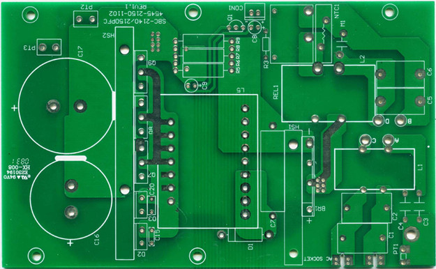
Four-layer PCB board drawing process
Release date:2022-12-07 16:31:25 Number of views:106
Four-layer PCB board drawing process and precautions

Four-layer PCB board drawing process:
1. Draw the circuit schematic diagram and generate the network table.
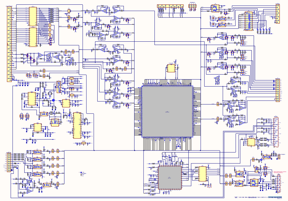
Among them, the process of drawing the schematic diagram involves the drawing of the components and the drawing of the four -layer pcb design of the package. It is basically not a problem to master these two drawing schematic diagrams. For the exclusion of errors and warnings, general problems should be able to be solved. Complex schematics can be drawn using hierarchical schematics.
The shortcut keys used here: CTRL+G (set the network table spacing) four-layer pcb design , CTRL+M (measure the distance between two points)
2. Planning the circuit board
How many layers to draw? Are components placed on one side or two sides? What is the board size? and many more
3. Set various parameters
Layout parameters and layer parameters are basically in accordance with the default of the system, and only a small number of parameters need to be set.
4. Load the netlist and component package
->.
Note: If there is an error in the process of drawing the schematic diagram, but the layout of the PCB has been done, and you want to correct the error without affecting the PCB layout, then this step is also performed, only in the last item. Do not check Add in front of the item! Do not check! Do not check! Say important things three times. Otherwise it will re-layout, which is a pain! !
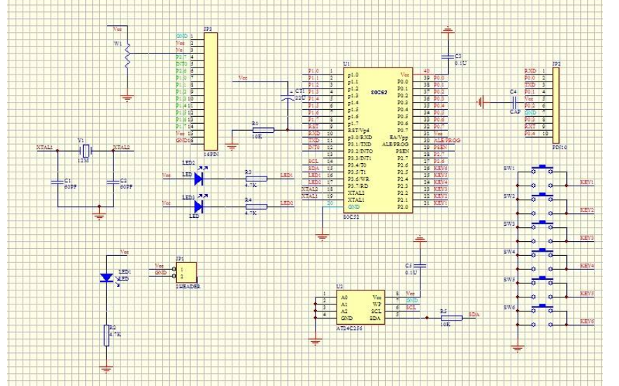
The netlist is the interface between the circuit schematic diagram editing software and the printed circuit board PCB design software. Only after loading the netlist, can the circuit board be automatically routed.
5. Layout of components
In most cases it is manual layout, or a combination of automatic and manual.
If you want to place components on both sides: select the component and press the left mouse button, and then press the L key; or click the component on the PCB interface, and modify its property to .
Notice:
Components are evenly arranged for mounting, plug-in, and soldering operations. The text is placed on the current character layer, and the position is reasonable. Pay attention to the orientation, avoid being blocked, and facilitate production.
6. Wiring
Automatic wiring, manual wiring (plan the layout before wiring, cooperate with the internal electrical layer, and hide the internal electrical layer for wiring. The inner electrical layer is usually a whole piece of copper film, and the pad with the same network name as the copper film is in the When passing through the internal electrical layer, the system will automatically connect it to the copper film. The connection form of the pad/via to the internal electrical layer, as well as the copper film and other pads that do not belong to the network and the safety distance can be specified in the rules. set up.
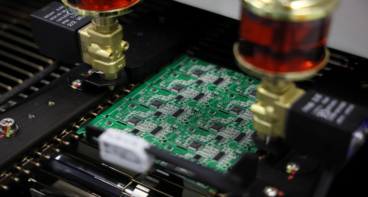
KFPCBA is a professional PCB manufacturer in China. We continue to invest heavily in maintaining state-of-the-art production processes and increasing productivity to be able to meet customer demand for high volumes of advanced circuit boards.
Comment on this article here
-
No comment

Ripple
Hi everyone, I'm Ripple, Sales Director of KFPCBA Tech Ltd. If you are looking for a one-stop PCB and PCB assembly manufacturer in China, KFPCBA is your best choice! Please feel free to contact our team! Thanks!
Contact me now
Relevant content you may be interested in
Related articles


