


 tel:+86-18825224069
 email:
 address:201, Factory 6, Longhui Industrial Park, Fuqiao 3rd District, Xinhe Community, Fuhai Street, Baoan District, Shenzhen china
Exploring the PCB Assembly Manufacturing Process
Release date:2023-05-26 11:24:41 Number of views:0
PCB assembly is a critical process that involves assembling electronic components onto printed circuit boards (PCBs). It is an intricate process that requires specialized skills, technical expertise, and state-of-the-art equipment. PCB assembly manufacturing is an essential aspect of the electronics industry, and it plays a vital role in ensuring that electronic devices are functional and reliable. In this article, we will explore the PCB assembly manufacturing process, from the design stage to the final assembly. We will take a closer look at the various steps involved in the process and the critical factors that contribute to the success of the final product. Whether you are an electronics enthusiast or a professional in the industry, this article will provide you with valuable insights into the PCB assembly manufacturing process. So, let's dive in and explore the world of PCB assembly manufacturing!

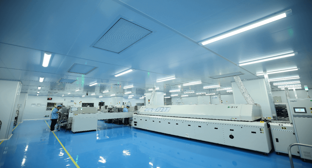
PCB smt production line
The History of PCB Assembly Manufacturing
The history of PCB assembly manufacturing dates back to the early 1900s, when the first PCB was invented. At that time, PCBs were simple, and the assembly process was manual. However, as the electronics industry grew, the demand for more complex PCBs increased, leading to the development of automated assembly processes. In the 1960s, the first surface mount technology (SMT) assembly process was developed, which revolutionized the industry. SMT allowed for the production of smaller and more complex PCBs, leading to the creation of more advanced electronic devices. Today, PCB assembly manufacturing is a highly specialized industry that uses advanced equipment and processes to produce high-quality PCBs.
Types of PCB Assembly Processes
There are two main types of PCB assembly processes: SMT and through-hole. SMT is the most commonly used PCB assembly process and involves placing surface-mounted components onto the PCB. Through-hole assembly, on the other hand, involves inserting components into holes drilled into the PCB. SMT is preferred for its smaller size, higher component density, and lower manufacturing costs. Through-hole assembly, on the other hand, is preferred for its higher mechanical strength and better electrical conductivity. Both processes have their advantages and disadvantages and are used depending on the requirements of the final product.
SMT vs. Through-hole Assembly
SMT and through-hole assembly differ in their component placement and soldering processes. In SMT, components are placed directly onto the surface of the PCB and are soldered using a reflow oven. In through-hole assembly, components are inserted into holes drilled into the PCB and are soldered using a wave soldering machine. SMT is preferred for its smaller size and higher component density, while through-hole assembly is preferred for its higher mechanical strength and better electrical conductivity. However, both processes have their advantages and disadvantages and are used depending on the requirements of the final product.
PCB Design and Layout Considerations for Assembly
PCB design and layout play a critical role in the success of the PCB assembly process. Designers must consider several factors when designing the PCB, including component placement, trace routing, and clearance. Components must be placed in a way that allows for easy access during assembly, and trace routing must be optimized to reduce the risk of signal interference. Clearance must also be considered to prevent component overlap and to ensure that there is enough space for proper soldering. By considering these factors, designers can create PCBs that are easy to assemble and of high quality.
The PCB Assembly Process Steps
The Surface Mount Technology (SMT) assembly process is a common method used to assemble electronic components onto a printed circuit board (PCB). Here are the typical steps involved in the PCB SMT assembly process:
1.Stencil Creation: A stencil is created that defines the solder paste pattern. This stencil is usually made of stainless steel and contains openings where the solder paste will be deposited on the PCB.
2.PCB Preparation: The bare PCB is inspected for defects, cleaned, and prepared for the assembly process. This may involve cleaning the surface to remove any contaminants and ensuring the PCB is properly aligned and secured.
3.Solder Paste Application: Solder paste, a mixture of solder alloy and flux, is applied to the pads on the PCB using the stencil. This paste acts as an adhesive to hold the components in place during the soldering process.
4.Pick and Place: Automated pick and place machines are used to accurately place the surface mount components onto the solder paste. These machines use vision systems to identify component positions and precisely position them on the PCB. The components are usually supplied on reels or trays and are picked up by the machine's nozzle and placed on the PCB.
5.Reflow Soldering: The PCB with the components and solder paste is then subjected to a reflow soldering process. The PCB is passed through a conveyor oven where it is heated to a specific temperature profile. This causes the solder paste to melt and form a reliable electrical connection between the components and the PCB pads. The solder joints re-solidify as the PCB exits the oven.
6.Inspection: After soldering, the PCB assembly undergoes inspection to identify any defects such as misaligned components, solder bridges, or missing solder joints. Automated optical inspection (AOI) systems and X-ray inspection may be used to ensure the quality of the assembly. This step helps identify any soldering defects that may require rework or repair.
7.Rework and Repair: If any defects are found during inspection, rework or repair processes are performed to rectify the issues. This may involve removing and replacing components, correcting solder joints, or addressing any other identified issues.
8.Cleaning: Once the assembly is inspected and any necessary rework is completed, the PCB assembly may undergo a cleaning process to remove any residual flux or contaminants. This step helps improve the reliability and longevity of the assembly.
9.Testing and Quality Assurance: After cleaning, functional testing is conducted to verify the performance of the PCB assembly. This may involve various tests such as power-on testing, boundary scan testing, in-circuit testing (ICT), or functional testing using specialized equipment. Quality assurance measures are implemented to ensure the overall quality and reliability of the PCB assembly.
10.Final Assembly: After successful testing, any additional steps such as conformal coating, potting, or enclosure assembly may be performed depending on the specific requirements of the PCB assembly.
11.Packaging and Shipping: The completed PCB assemblies are packaged according to the customer's specifications and prepared for shipping.
It's important to note that the specific steps and processes may vary depending on factors such as the complexity of the PCB design, the size of the production run, and the manufacturing capabilities of the assembly facility.
PCB Assembly Equipment and Tools
PCB assembly requires specialized equipment and tools to ensure that the process runs smoothly. Some of the essential equipment used in PCB assembly include pick and place machines, reflow ovens, soldering irons, wave soldering machines, and inspection equipment. These machines and tools are designed to handle the delicate components used in PCB assembly and to ensure that the process is efficient and of high quality.
Quality Control and Testing in PCB Assembly
Quality control and testing are critical aspects of the PCB assembly process, ensuring that the final product is of high quality and meets the required standards. Inspection and testing are carried out during the assembly process to identify any defects or issues that may arise. Once the assembly is complete, the PCB is thoroughly tested to ensure that it is functioning correctly. Quality control measures are also put in place to ensure that the PCB assembly process is consistent and of high quality.

Quality Control and Testing
Common PCB Assembly Mistakes and How to Avoid Them
Like any manufacturing process, PCB assembly is prone to errors and mistakes. Some of the common mistakes that occur during PCB assembly include incorrect component placement, insufficient soldering, and defective components. These mistakes can lead to the failure of the final product and can be costly to correct. To avoid these mistakes, it is essential to have a well-defined assembly process, quality control measures, and skilled technicians. Regular training and calibration of equipment and tools can also help to minimize errors and ensure that the final product is of high quality.
The Future of PCB Assembly Manufacturing
The future of PCB assembly manufacturing is expected to be driven by advancements in technology and increased demand for more complex electronic devices. New materials, such as flexible PCBs and conductive inks, are being developed, which will lead to the creation of more advanced electronic devices. Automation and robotics are also expected to play a more significant role in the assembly process, leading to increased efficiency and lower costs. Overall, the future of PCB assembly manufacturing is bright, and the industry is expected to continue growing in the coming years.
Conclusion
PCB assembly manufacturing is a critical process that plays a vital role in the electronics industry. It is an intricate process that requires specialized skills, technical expertise, and state-of-the-art equipment. In this article, we have explored the various steps involved in the PCB assembly process, from the design stage to the final assembly. We have also discussed the critical factors that contribute to the success of the final product, including PCB design and layout, equipment and tools, quality control, and testing. By understanding the PCB assembly process, we can appreciate the complexity and importance of this vital industry.
Comment on this article here
-
No comment

Ripple
Hi everyone, I'm Ripple, Sales Director of KFPCBA Tech Ltd. If you are looking for a one-stop PCB and PCB assembly manufacturer in China, KFPCBA is your best choice! Please feel free to contact our team! Thanks!
Contact me now
Relevant content you may be interested in
Related articles


