


 tel:+86-18825224069
 email:
 address:201, Factory 6, Longhui Industrial Park, Fuqiao 3rd District, Xinhe Community, Fuhai Street, Baoan District, Shenzhen china
Some Layout Design Tips For Custom Circuit Board Circuit Board Design
Release date:2022-11-29 14:15:40 Number of views:88
Some layout design tips for custom circuit board circuit board design ! (one)
On the basis of fully analyzing the circuit and determining the key circuit, the circuit must also be properly arranged on the printed board. For example, for digital circuits, high-speed circuits (such as clock circuits, high-speed logic circuits, etc.), medium and low-speed logic circuits, and UO circuits should be arranged in different areas, and the interference source and the sensitive circuit should be separated as much as possible in space, so that the interference source Radiation interference to sensitive circuits is greatly reduced. 2 Printed board anti-interference design: The purpose of PCB anti-interference design is to reduce the electromagnetic radiation of the PCB board and the crosstalk between the circuits on the PCB board. In addition, the ground wire design of the PCB also directly affects the common-mode voltage radiation of the 1/0 cable. Therefore, the anti-interference design of PCB is of great significance to reduce the electromagnetic information radiation of the system.
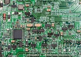
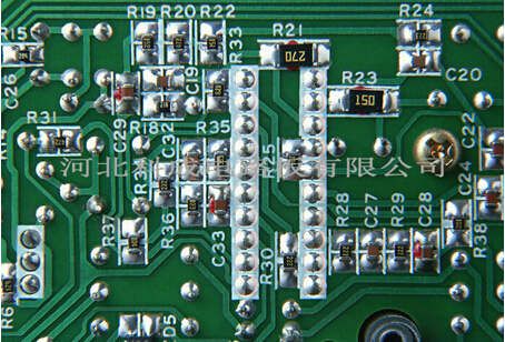
2.1 PCB layout design: The density of the printed circuit board (PCB) is getting higher and higher, and the quality of the PCB design has a great influence on the anti-interference ability, so the layout of the PCB is in a very important position in the design.
PCB circuit board design is a thought-provoking job. Whoever has a close mind and high experience can design a good board. Hunan Custom Circuit Board Processing Factory
PCB circuit board is the basic electronic component of all electronic circuit design , and the design of PCB circuit board is also a must for makers. The function of PCB is not only to combine scattered components, but also to ensure the regularity of circuit design, which well avoids the confusion and errors caused by manual wiring and wiring. 1. There must be a reasonable direction; 2. Choose a good grounding point: the grounding point is often important; 3. Reasonably arrange the power filter/decoupling capacitor; The number of holes, solder joints and line density; If you can fully understand and master the above PCB circuit board design considerations, you can greatly improve design efficiency and product quality. Correcting existing errors during production will save a lot of time and cost, and save rework time and material input. In the design of high-speed PCB circuit boards, seemingly simple vias often bring great negative effects to the circuit design.
Use reasonable wiring design to realize heat dissipation. Because the resin in the board has poor thermal conductivity, and copper foil lines and holes are good conductors of heat, increasing the remaining copper foil and increasing heat conduction holes are the main means of heat dissipation. To evaluate the heat dissipation capability of PCB , it is necessary to calculate the equivalent thermal conductivity (nine eq) of the composite material composed of various materials with different thermal conductivity—the insulating substrate for PCB circuit boards. The devices on the same printed board should be arranged according to their calorific value and heat dissipation degree as much as possible. Devices with small calorific value or poor heat resistance (such as small signal transistors, small-scale integrated circuits, electrolytic capacitors, etc.) should be placed in the cooling airflow. Upstream (inlet), devices with high heat generation or good heat resistance (such as power transistors, large-scale integrated circuits, etc.) are placed downstream of the cooling airflow.
Electromagnetic compatibility (EMC) refers to the ability of an electronic system to work normally in accordance with the design requirements in a specified electromagnetic environment. The electromagnetic interference suffered by the electronic system not only comes from the radiation of the electric field and the magnetic field, but also has the influence of the common impedance of the line, the connection between the wires and the circuit structure. When developing and designing circuits, we also hope that the designed printed circuit boards will not be affected by external interference as much as possible, and it will interfere with other electronic systems as little as possible. There are many factors that affect the anti-interference performance of printed boards, including the thickness of copper foil, the width and length of printed wires, the crosstalk between adjacent wires, the rationality of the layout of components in the board, and the common impedance of wires, Electromagnetic fields generated by wires and components in space, etc. Now the thickness (through hole depth) of a normal 6-layer PCB circuit board is about 50Mil, so the diameter of the drill hole that the PCB manufacturer can provide is as small as 8Mil.
There are several approaches to solving PCB-based product design problems, each of which varies widely. But which method is faster? which kind? Which consumes less project resources? All of these issues have important implications for the success of the project. There are two options for PCB designers: first, you can design freely, and then find a production chain to realize this design. Second, understand your production chain and optimize your design to suit the manufacturer's strengths while maintaining the desired functionality. Here, designers share five strategies that can help you plan ahead without adding weeks or unnecessary cost to the design process. 1. Research and select suppliers early in the design; 2. Reduce costs and optimize performance before layout; 3. Develop your layout into a "sweet pot" for the manufacturing plant; 4. Use supplier DFM tools to verify your Layout production capacity; 5. Manage prototype cost and hidden cost
Buried holes refer to connection holes located in the inner layer of the printed circuit board, which do not extend to the surface of the circuit board. Anhui customized circuit board brand
Electromagnetic Interference (System Destruction) Controlling all of the above units, while shielding the entire PCB or the noise-sensitive and noise-generating parts helps to control EMI. CHINA Custom Circuit Board Processing Factory
In this era of fabless IC companies, it's not surprising that many engineers are truly ignorant of the steps and chemistry involved in generating a circuit board from their design files. This lack of practical knowledge often leads novice designers to make unnecessarily complex design choices. For example, a common mistake that novices make is to design the pcb layout with extremely precise dimensions, that is, to use orthogonal wires associated with a tight grid, and find that not every pcb circuit board processing factory can produce in A design capable of maintaining sufficient reliability during its field service life. A factory with these capabilities may not be able to offer economical pcb prices. Does the design really need to be that complicated? Can a pcb layout be designed on a larger grid, thereby reducing pcb cost and increasing reliability? Other pitfalls that novice designers encounter include via sizes that are too small and blind and buried vias. These advanced via structures are the product of powerful tools in the PCB designer's toolbox, but their effectiveness is highly situation-specific. Just because they exist in the toolbox doesn't mean they should be used. Bert's "Design Notes" blog has this to say about via aspect ratios: "A via with an aspect ratio of 6:1 is a good way to ensure that your PCB can be fabricated anywhere." For most designs In general, with a little thought and planning, these HDI features can be avoided entirely, again saving cost and improving the manufacturability of the design. Hunan Custom Circuit Board Processing Factory
Comment on this article here
-
No comment

Ripple
Hi everyone, I'm Ripple, Sales Director of KFPCBA Tech Ltd. If you are looking for a one-stop PCB and PCB assembly manufacturer in China, KFPCBA is your best choice! Please feel free to contact our team! Thanks!
Contact me now
Relevant content you may be interested in
Related articles


