


 tel:+86-18825224069
 email:
 address:201, Factory 6, Longhui Industrial Park, Fuqiao 3rd District, Xinhe Community, Fuhai Street, Baoan District, Shenzhen china
PCB Layout Of Photovoltaic Power Supply And Layout Copper Pours
Release date:2022-12-07 16:42:17 Number of views:103
PCB layout of photovoltaic power supply and layout of PCB traces and copper pours
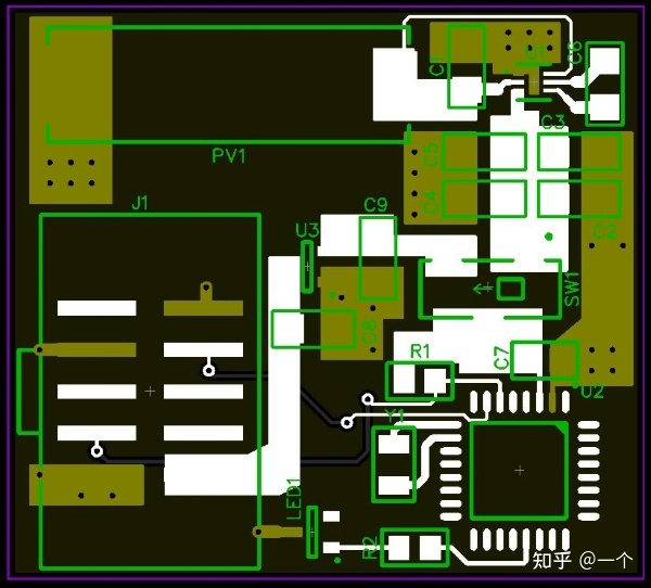
PCB layout of photovoltaic power supply circuit
My goal in this project is to create a very simple, very compact circuit that can power a microcontroller based embedded system. The circuit is only active during times of sufficient lighting, as the design includes no capacitors or batteries to store surplus energy.
In this article double layer pcb design , I will understand the PCB layout of the circuit from the power supply schematic.
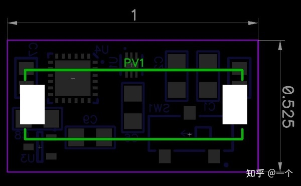
PCB layout of photovoltaic power supply
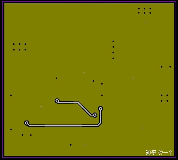
The image below shows the layout of the top and bottom of the PCB. All components and most traces and copper pours are on the top; the bottom is mostly the ground plane.
PCB size
The microcontroller is an EFM8 Bee from Labs, and the (relatively) large connector on the left provides a direct connection to a USB debug adapter. This type of connector consumes a considerable amount of PCB space and makes the overall design appear larger than it is.
The image below shows the dimensions of the PCB in inches. The shorter horizontal dimension is my attempt to estimate how small the board could be if the debug connectors were removed (and other components rearranged) .
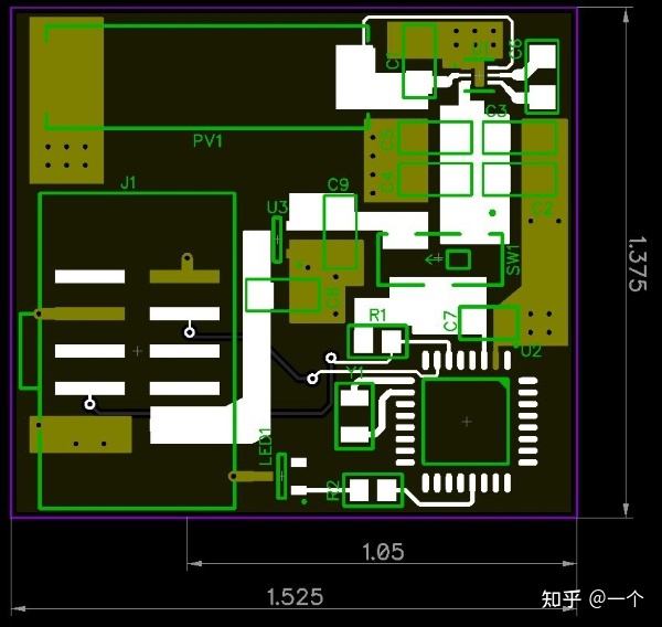
So my guess is that the double board with all components on one side is probably less than 1.5 square inches. I'd say that's pretty cool, especially considering we're talking about a two-layer PCB.
Also, I don't think I'm losing any performance by using two layers instead of four, since the bottom is pretty much a solid ground plane and the top has plenty of room for wide power lines and wide ground connections (also because the microcontroller will run at a very low frequency).
Small and compact, but it could be even smaller
Here are some other ways you can reduce the size of this board:
● I chose the larger passive component ICs (0805 and 1206) because they are easier to assemble. If you plan on assembling the board, you might consider using a 0603 or even a 0402 (you may find acceptable 2.2µF caps in a 0402 package, but for 0.1µF caps and resistors you can use 0402).
● I chose a larger package for the microcontroller; it was a 9 mm x 9 mm QFP32. The 32-pin leadless package was significantly smaller (5 mm x 5 mm), and there was also a 24-pin leadless Leaded package, smaller size (4 mm × 4 mm). It seems to me that most applications built around this power supply don't need more than a handful of I/O pins, so a 24-pin package is probably the way to go. The reason I'm using a 32-pin device is that this microcontroller doesn't come in any other leaded (i.e. non-leaded) package.
● I provided a 32.768 kHz crystal for the real time clock application; it is about the size of an 0805 component. The microcontroller has an internal low power oscillator that is very low (±10%), so you can omit the crystal if you don't need timing.
● Charge-pump switching regulators currently have four 2.2µF output capacitors, but only one is required.
● The LEDs and their accompanying resistors are for debugging only; they can be omitted in the final design.
● You might think that you can eliminate all the circuitry (switch, LDO, and two capacitors) associated with debugging the power supply. I do not recommend this as solar power is not a convenient power source for firmware development and testing.
double sided selection
The last item on how to make a smaller list is to have components on the top and bottom of the board. As I was writing this I was starting to wonder if the whole circuit would fit in the area corresponding to the size of the solar cell so that you could design a board with just the top solar cell and something else on the bottom. I decided to remove some unnecessary components from the schematic and try out the idea, here's what I found (dimensions are in inches):
This is a rough approximation, but, as you can see with the double layer pcb design , we are very close to our goal of cramming all the circuitry into the PCB space that the solar cell takes up.
To create this component placement, I eliminated three of the four output capacitors, the crystal, the LED, and the LED's resistor. I also switched the microcontroller package to a QFN24. The passive components are still 1206s and 0805s, but these larger packages make up for your need for some way to connect the microcontroller to the debug adapter. Of course there isn't much room for routing, but if you can use a four layer board (and still have enough space on top below the solar cells), I don't think it's a serious hindrance.
in conclusion
We've discussed the PCB layout for a solar microcontroller board I recently designed, and we've also looked at an example of a more space-optimized implementation where the PCB's dimensions are close to those of a solar cell. If you have any experience with space-constrained design for low-power embedded devices, please feel free to share your thoughts in the comments.
Comment on this article here
-
No comment

Ripple
Hi everyone, I'm Ripple, Sales Director of KFPCBA Tech Ltd. If you are looking for a one-stop PCB and PCB assembly manufacturer in China, KFPCBA is your best choice! Please feel free to contact our team! Thanks!
Contact me now


