


 tel:+86-18825224069
 email:
 address:201, Factory 6, Longhui Industrial Park, Fuqiao 3rd District, Xinhe Community, Fuhai Street, Baoan District, Shenzhen china
Takes You To Design And Route Multilayer Printed Circuit Boards
Release date:2022-12-08 17:33:22 Number of views:106
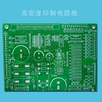
ShenzhenThe circuit board factory takes you to design and route multilayer printed circuit boards
What is your understanding of the design and wiring of multilayer printed circuit boards? Let Shenzhen Circuit Board Factory take you to summarize the design and wiring of multilayer printed circuit boards today!
The emergence of multilayer printed circuits provides a solution for interconnecting small components into complex systems. The volume and weight occupied by ordinary wiring are greater than the volume and weight of the components it interconnects , which is very disproportionate. Since the multilayer printed circuit) is a multi-plane wire structure, it is possible to reduce the volume and weight of the interconnection line to a level commensurate with the volume and weight of the interconnected components. How much volume and weight can be reduced depends on the specific package design.
The application field that best embodies the advantages of multilayer printed circuits is to interconnect integrated circuits. Integrated circuits can also be interconnected by other wiring techniques, such as welding matrix, point-by-point wiring, and double-sided printed boards. However, packaging with these methods requires sacrificing interconnect density, increasing volume and weight. Integrated circuits and multilayer printed circuit boards can greatly reduce the overall volume and weight of the entire system.
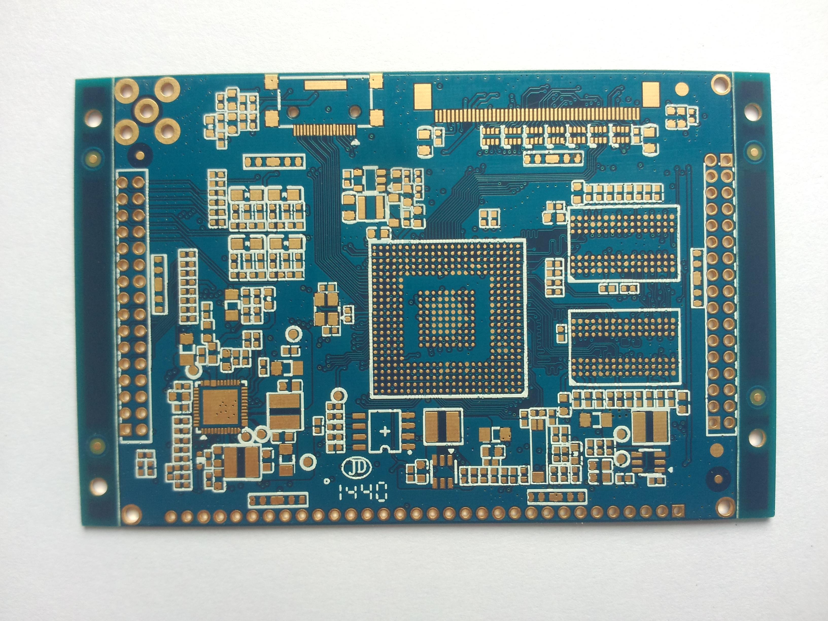
Another obvious application for multilayer boards is to accommodate heat distribution and cooling issues for systems using integrated circuits. Due to the multi-layer structure, all interconnects can be placed on the inner layers, and heat sinks made of thick solid copper or other materials can be placed on the outer surfaces, so that the components can be mounted directly on the metal surface
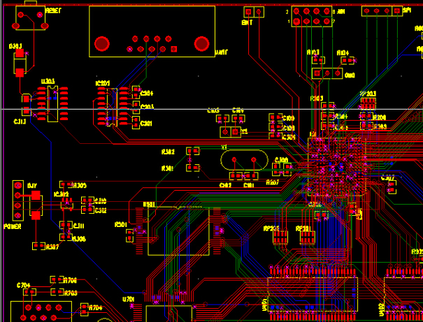
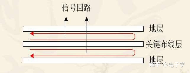
The third feature of multilayer printed circuit boards is that they can be added to the ground plane or shielding plane. Solid copper surface etched with clearance holes, can be placed anywhere within the multilayer board structure. Clearance holes are etched in areas of the copper that do not require joints. These copper surfaces can be used to eliminate the electrical coupling between key circuits to minimize noise interference or crosstalk, and can also be used to shield some key circuits inside or outside the printed board or interfere with the entire printed board. Some of these copper surfaces can be placed on a printed board or used for power distribution. This characteristic of multilayer printed boards offers an interesting possibility. At the same time, in many cases , it is the only solution to some interconnection problems. In high-frequency circuits, the ground plane characteristics of multilayer boards play an important role.
Multilayer printed wiring has achieved the expected development, and with the emergence of more complex semiconductor devices LSI, it will continue to develop so that even system designers should be fully familiar with its potential and limitations. The new generation of electronic systems requires increasingly higher interconnect complexity and interconnect density - the development of higher operating frequencies is an undoubted trend, requiring even a single wire to be extremely carefully designed. The length, width, position and relationship of wires, spacing, dielectric materials, etc. are all interrelated, and in many cases, they have a significant impact on the signal transmission, noise figure, pulse waveform, and other electrical parameters of the system. Therefore, not only the electrical designer in electronic packaging but also the system designer is involved more deeply.
How about it? Now you have a certain summary and overview of the design and wiring of multilayer printed circuit boards! Bits of learning gather into the sea!
Comment on this article here
-
No comment

Ripple
Hi everyone, I'm Ripple, Sales Director of KFPCBA Tech Ltd. If you are looking for a one-stop PCB and PCB assembly manufacturer in China, KFPCBA is your best choice! Please feel free to contact our team! Thanks!
Contact me now
Relevant content you may be interested in
Related articles


